Appendix B. System address maps
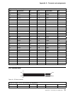
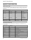
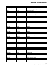
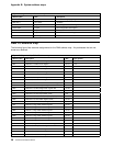
Figure 34 (Page 2 of 3). I/O address map
Address (Hex) Size Description
0080 1 byte POST checkpoint register during POST only
008F 1 byte Refresh page register
0080–008F 16 bytes ICH1, DMA page registers
0090–0091 15 bytes General I/O locations — available to PCI bus
0092 1 byte PS/2 keyboard controller registers
0093–009F 15 bytes General I/O locations
00A0–00A1 2 bytes Interrupt controller 2
00A2–00BF 30 bytes APM control
00C0–00DF 31 bytes DMA 2
00E0–00EF 16 bytes General I/O locations — available to PCI bus
00F0 1 byte BX, Coprocessor Error Register
00F1–016F 127 bytes General I/O locations — available to PCI bus
0170–0177 8 bytes Secondary IDE channel
01F0–01F7 8 bytes Primary IDE channel
0200–0207 8 bytes Available
0220–0227 8 bytes SMC 37C673, Serial port 3 or 4
0228–0277 80 bytes General I/O locations — available to PCI bus
0278–027F 8 bytes SMC 27C673, LPT3
0280–02E7 102 bytes Available
02E8–02EF 8 bytes SMC PC37C673, Serial port 3 or 4
02F8–02FF 8 bytes COM2
0338–033F 8 bytes SMC PC37C673, Serial port 3 or 4
0340–036F 48 bytes Available
0372–0375 4 bytes Available
0376–0377 2 bytes IDE channel 1 command
0378–037F 8 bytes LPT2
0380–03B3 52 bytes Available
03B4–03B7 4 bytes Video
03BA 1 byte Video
03BC–03BE 16 bytes LPT1
03C0–03CF 16 bytes Video
03D4–03D7 4 bytes Video
03DA 1 byte Video
03D0–03DF 11 bytes Available
03E0–03E7 8 bytes Available
03E8–03EF 8 bytes COM3 or COM4
03F0–03F5 6 bytes Diskette channel 1
03F6 1 byte Primary IDE channel command port
03F7 (Write) 1 byte Diskette channel 1 command
03F7, bit 7 1 bit Diskette disk change channel
03F7, bits 6:0 7 bits Primary IDE channel status port
03F8–03FF 8 bytes COM1
0400–047F 128 bytes Available
Appendix B. System address maps 37


