


Appendix B. System address maps
Appendix B. System address maps
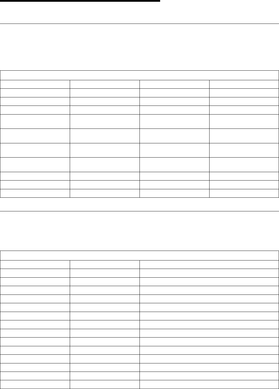
System memory map
The first 640 KB of system board RAM is mapped starting at address hex 0000000. A 256 byte area and
a 1 KB area of this RAM are reserved for BIOS data areas. Memory can be mapped differently if POST
detects an error.
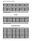
Input/output address map
The following figure lists resource assignments for the I/O address map. Any addresses that are not
shown are reserved.
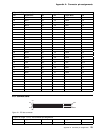
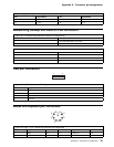
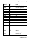
Figure 33. System memory map
Address range (decimal) Address range (hex) Size Description
0 K – 512 K 00000–7FFFF 512 KB Conventional
512 K – 639 K 80000–9FBFF 127 KB Extended conventional
639 K – 640 K 9FC00–9FFFF 1 KB Extended BIOS data
640 K – 767 K A0000–BFFFF 128 KB Dynamic video memory
display cache
768 K – 800 K C0000 to C7FFF 32 KB Video ROM BIOS
(shadowed)
800 K – 896 K C8000–DFFFF 96 KB PCI space, available to
adapter ROMs
896 K – 1 MB E0000–FFFFF 128 KB System ROM BIOS (main
memory shadowed)
1 MB – 16 MB 100000–FFFFFF 15 MB PCI Space
16 MB – 4095.872 MB 1000000–FFF7FFFF 4079.5 MB MB PCI Space (positive decode)
FFF80000 –FFFFFFFF 512 KB System ROM BIOS
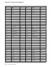
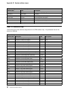
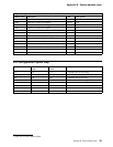
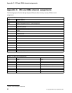
Figure 34 (Page 1 of 3). I/O address map
Address (Hex) Size Description
0000–000F 16 bytes DMA 1
0010–001F 16 bytes General I/O Locations — available to PCI bus
0020–0021 2 bytes Interrupt controller 1
0022–003F 30 bytes General I/0 locations — available to PCI bus
0022–002F 2 bytes SMC SIO index/data register
0040–0043 4 bytes Counter/timer 1
0044–00FF 28 bytes General I/0 locations — available to PCI bus
0060 1 byte Keyboard controller byte - reset IRQ
0061 1 byte PIIX4, System port B
0064 1 byte Keyboard controller, CMD/STAT byte
0070, bit 7 1 bit Enable NMI
0070, bits 6:0 1 bit Real time clock, address
0071 1 byte Real time clock, data
0072–007F 14 bytes General I/O locations — available to PCI bus
36 Copyright IBM Corp. September 1999