


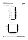
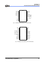

EM78M611E
Universal Serial Bus Series Microcontroller
10 •
••
•
Product Specification (V1.1) 11.22.2006
(This specification is subject to change without further notice)
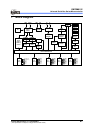
8.2.2 Operation Registers
The following subsections describe each of the Operation Registers of the Special
Purpose Registers. The Operation Registers are arranged according to the order of the
registers’ address. Note that some registers are read only, while others are both
readable and writable.
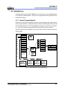
8.2.2.1 R0 (Indirect Addressing Register) Default Value: (0B_0000_0000)
R0 is not a physically implemented register. Its major function is as an indirect
addressing pointer. Any instruction using R0 as a pointer actually accesses data
pointed by the RAM Select Register (R4).
8.2.2.2 R1 (Timer / Clock Counter) Default Value: (0B_0000_0000)
The TCC register is an 8-bit timer or counter. It is readable and writable as any other
register. The Timer module will be incremented after execution of every instruction
cycles. User can work around this by writing an adjusted value. The Timer interrupt is
generated when the R1 register overflows from FFh to 00h. This overflow sets bit TCIF
(RF[0]). The interrupt can be masked by clearing bit TCIE (IOCF[0]). After Power-on
reset and Watchdog reset, the initial value of this register is 0x00.
8.2.2.3 R2 (Program Counter & Stack) Default Value: (0B_0000_0000)
The EM78M611E Program Counter is a 13-bit register that allows accessing of the 6k
words of the Program Memory with 8 level stacks. The eight LSB bits, A0~A7, are
located at R2, while the three MSB bits, A12~A10, are located at R3. The Program
Counter is cleared after Power-on reset or Watchdog reset. The first instruction that is
executed after a reset is located at address 00h.