


29
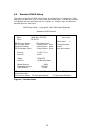
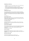
4.7 Advanced Chipset Features
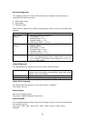
CMOS Setup Utility – Copyright © 1984 – 2000 Award Software
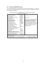
Advanced Chipset Features
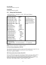
DRAM Timing Selectable By SPD
CAS Latency Time 1.5
Active to Precharge Delay 7
DRAM RAS# to CAS# Delay 3
DRAM RAS# Precharge 3
Memory Frequency For AUTO
System BIOS Cacheable Enabled
Video BIOS Cacheable Disabled
Memory Hole At 15M-16M Disabled
Delayed Transaction Enabled
AGP Aperture Size 64MB
** Onboard Display Cache Setting **
On-chip VGA Enabled
Flash BIOS Disabled
Item Help
_______________________
Menu Level ¾
↑↓←→Move Enter: Select +/-/PU/PD: Value F10: Save ESC: Exit
F1: General Help
F5: Previous Values F6: Fail-safe defaults F7: Optimized Defaults
This section allows users to configure the system based on the specific features of
the installed chipset. This chipset manages bus speeds and accesses to system
memory resources, such as DRAM and the external cache. It also coordinates
communications between the conventional ISA bus and the PCI bus. It must be
stated that these items should never need to be altered. The default settings
have been chosen because they provide the best operating conditions for the
system.
DRAM Timing Selectable
The first chipset settings deal with CPU access to dynamic random access
memory (DRAM). The default timings have been carefully chosen and should
only be altered if data is being lost. Such a scenario might well occur if the
system had mixed speed DRAM chips installed so that greater delays may be
required to preserve the integrity of the data held in the slower memory chips.
CAS Latency Time
When synchronous DRAM is installed, the number of clock cycles of CAS latency
depends on the DRAM timing.
The Choice: 1.5, 2, 2.5, 3.
DRAM Cycle Time Tras/Trc
Select the number of SCLKs for an access cycle.
The choice: 5/7, 6/8.