


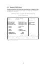
30
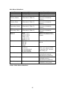
DRAM RAS# to CAS# Delay
• This field lets users insert a timing delay between the CAS and RAS strobe
signals.
• It is used when DRAM is written to, read from, or refreshed.
• Choice 2 means shorter delay which shortens the process of charging; and
choice 3 means longer delay which lengthens the process of charging.
• This field applies only if the synchronous DRAM is installed in the system.
The choice: 2, 3.
DRAM RAS# Precharge
If an insufficient number of cycles are allowed for the RAS to accumulate its
charge before DRAM refresh, the refresh may be incomplete and the DRAM may
fail to retain data. Fast gives faster performance; and Slow gives more stable
performance. This field applies only when synchronous DRAM is installed in the
system.
The choice: 2, 3.
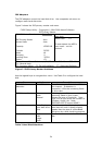
System BIOS Cacheable
Selecting Enabled allows caching of the system BIOS ROM at F0000h-FFFFFh,
resulting in better system performance. However, if any program writes to this
memory area, a system error may result.
The choice: Enabled, Disabled.
Video BIOS Cacheable
Select Enabled allows caching of the video BIOS, resulting in better system
performance. However, if any program writes to this memory area, a system
error may occur.
The Choice: Enabled, Disabled.
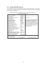
Memory Hole At 15M-16M
This area of system memory can be reserved for ISA adapter ROM. When this
area is reserved, it cannot be cached. The user information of peripherals that
requests this area of system memory usually discusses their memory
requirements.
The Choice: Enabled, Disabled.
Delay Transaction
The chipset has an embedded 32-bit posted write buffer to support delay
transactions cycles. Select Enabled to support compliance with PCI specification
version 2.1.
The Choice: Enabled, Disabled.
AGP Aperture Size (MB)
elect the on-chip video window size for VGA drive use.
The Choice: 4MB, 8MB, 16MB, 32MB, 64MB, 128MB, 256MB