


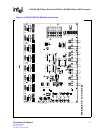

LXD9785 PQFP Demo Board with FPGA for SS-SMII (Fiber)-to-MII Conversion
Development Kit Manual 15
Document #: 249323
Revision #: 003
Rev. Date: January 24, 2002
4.3 Alternate MDIO Routing Configuration
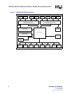
The MDIO and MDC signals may be routed either through the 40-pin connector for MII Port 0 (the
standard configuration) or through an RJ-11 connector (J2), as shown in Table 6. In either
configuration, the MII registers can be accessed for each port by setting the correct PHY address.
Refer to the LXT9785/9785E Data Sheet for specific register definitions and functions. The
standard configuration is to route MDIO through the Port 0 MII connector to the SmartBits Test
Box by setting the pins for JP1 and JP2 to 2 & 3.
Note: MDIO sectionalization is not supported on this demo board.
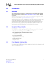
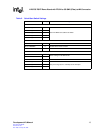
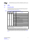
Table 5. PHY Address Configuration Settings (Switch S1)
Jumper / Label Description
S1-1 / ADD_0 Address <4:0> - Sets base address. Each port adds its port number (starting with 0)
to this address to determine its PHY address.
Switch “0” sets address bit to 0.
Switch “1” sets address bit to 10.
Note: To make all ports accessible within the 0 - 31 PHY address range, DO NOT
select a base address higher than 24.
Port 0 = Base + 0
Port 1 = Base + 1
Port 2 = Base + 2
Port 3 = Base + 3
Port 4 = Base + 4
Port 5 = Base + 5
Port 6 = Base + 6
Port 7 = Base + 7
S1-2 / ADD_1
S1-3 / ADD_2
S1-4 / ADD_3
S1-5 / ADD_4
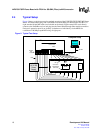
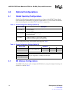
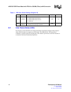
Table 6. MDIO Routing (Port 0)
Desired Configuration Jumper Setting Description
Route MDIO0 and MDC0
through MII
JP2
Jumper
Pins 2 & 3
Routes MDC0 through Port 0 MII Connector.
JP1
Jumper
Pins 2 & 3
Routes MDIO0 through Port 0 MII Connector.
Route MDIO0 and MDC0
through RJ-11
JP2
Jumper
Pins 1 & 2
Routes MDC0 through RJ-11 Connector J2.
JP1
Jumper
Pins 1 & 2
Routes MDIO0 through RJ-11 Connector J2.