


LXD9785 PQFP Demo Board with FPGA for SS-SMII (Fiber)-to-MII Conversion Development Kit Manual iii
Document #: 249323
Revision #: 003
Rev. Date: January 24, 2002
Contents
Contents
1.0 General Description.........................................................................................................................7
1.1 Features................................................................................................................................7
2.0 Introduction......................................................................................................................................9
2.1 Overview...............................................................................................................................9
2.2 Equipment Requirements .....................................................................................................9
2.3 Fiber Register Configuration.................................................................................................9
2.4 Typical Setup......................................................................................................................10
3.0 Quick-Start Checklist.....................................................................................................................12
4.0 Optional Configurations.................................................................................................................14
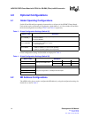
4.1 Global Operating Configurations ........................................................................................14
4.2 MII Address Configurations ................................................................................................14
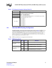
4.3 Alternate MDIO Routing Configuration ...............................................................................15
4.4 JTAG Test Signals..............................................................................................................16
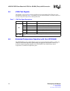
4.5 Extended Temperature Operation with the LXT9785HE ....................................................16
5.0 LEDs..............................................................................................................................................17
5.1 Direct Drive LEDs ...............................................................................................................17
5.2 Inter Frame Status LEDs ....................................................................................................18
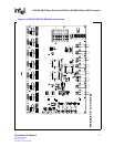
6.0 Board Schematics .........................................................................................................................19
7.0 Bill of Materials ..............................................................................................................................36
Figures
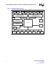
1 LXD9785 PQFP MII Demo Board.................................................................................................8
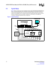
2 Typical Test Setup......................................................................................................................10
3 LXD9785/9785E SS-SMII Fiber Demo Board.............................................................................11
4 LXD9785 PQFP MII Demo Board Power (Fiber Board Revision A2) .........................................19
5 Control ........................................................................................................................................20
6 MII Ports 0 and 1 ........................................................................................................................21
7 MII Ports 2 and 3 ........................................................................................................................22
8 MII Ports 4 and 5 ........................................................................................................................23
9 MII Ports 6 and 7 ........................................................................................................................24
10 Fiber Ports 0 and 1 .....................................................................................................................25
11 Fiber Ports 2 and 3 .....................................................................................................................26
12 Fiber Ports 4 and 5 .....................................................................................................................27
13 Fiber Ports 6 and 7 .....................................................................................................................28
14 Caps ...........................................................................................................................................29
15 SS-SMII to MII ALTERA .............................................................................................................30
16 Clock Distribution........................................................................................................................31
17 Inter-Frame Status LEDs............................................................................................................32
18 Logic Analyzer ............................................................................................................................33
19 MDIO0 and MDC0 Fix ................................................................................................................34
20 MDIO1 and MDC1 Fix ................................................................................................................35