


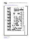
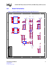

LXD9785 PQFP Demo Board with FPGA for SS-SMII (Fiber)-to-MII Conversion
14 Development Kit Manual
Document #: 249323
Revision #: 003
Rev. Date: January 24, 2002
4.0 Optional Configurations
4.1 Global Operating Configurations
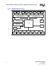
Switch S5 and S8 configure operating characteristics on all ports of the LXD9875 Demo Board.
Each switch can be set manually by toggling the switch either to 1 or 0. Set switches S5 and S8 to
the desired configuration according to Table 3 and Table 4 respectively.
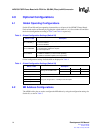
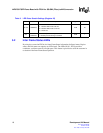
Global configuration settings for Switch S8 are displayed in Table 4.
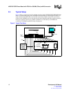
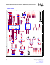
4.2 MII Address Configurations
The ADDR <4:0> pins are used to configure the MII address by using the configuration settings for
Switch S1, as seen in Table 5.
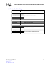
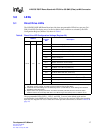
Table 3. Global Configuration Settings (Switch S5)
Switch / Label Description
S5-1 / PAUSE_0
Pause - Enable Pause capability on all ports.
1 = Pause enabled.
0 = Pause disabled.
S5-2 / PWRDWN
Power-Down - Enable global power-down mode.
1 = Power-Down enabled on all ports.
0 = Normal operation.
S5-3 / MDDIS
Management Disable - Disables MDIO Access.
1 = MDIO is disabled. (no read or write capability).
0 = MDIO is read/write capable (normal operation).
Table 4. Global Configuration Settings (Switch S8)
Switch / Label Description
S8-1 / ModeSel 0
Settings for SS-SMII mode.
ModeSel1 ModeSel0 Mode
S8-2 / ModeSel 1 1 0 SS-SMII
S8-3 /Section Enables Section mode: 1x8 or 2x4.
S8-4 / CFG_3
Sets port configuration to 100 Mbps and Full-Duplex.S8-5 / CFG_2
S8-6 / CFG_1