


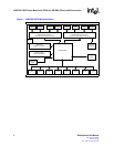
LXD9785 PQFP Demo Board with FPGA for SS-SMII (Fiber)-to-MII Conversion
16 Development Kit Manual
Document #: 249323
Revision #: 003
Rev. Date: January 24, 2002
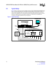
4.4 JTAG Test Signals
The boundary scan test port is accessed via JP3 for board- level testing. The JTAG test signal
descriptions are shown in Table 7. The BSDL file for the LXT9785/9785E is available on the Intel
web site at http://developer.intel.com/design/network/.
4.5 Extended Temperature Operation with the LXT9785HE
The LXT9785HE provides reliable Ethernet transceiver functionality from -40
o
C to +85
o
C. Any
LXD9785 demo board supporting a QFP package can support an LXT9785HE mounted and
localized extended temperature applied to the LXT9785HE. The LXD9785 demo board
components are commercial temperature grade.
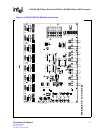
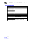
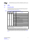
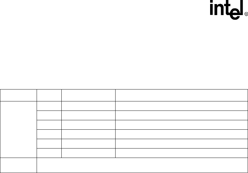
Table 7. JTAG Test Signal Descriptions
Jumper Pin# Symbol Description
JP3
1TRST#Test Reset. Input sourced by ATE
3TCKTest Clock. Input sourced by ATE.
5TMSTest Mode Select. Input sourced by ATE.
7TDOTest Data Output. Output sourced by the PHY.
8TDITest Data Input. Input sourced by the ATE.
2,4,6 GND Connected to system ground.
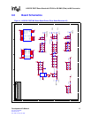
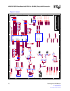
JP11 / PLD0
JP11 is used for FPGA debug and is not designated for evaluation of the LXT9785/9785E
device.