


SSI
EPS1U Power Supply Design Guide, V1.1
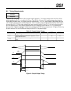
8.4 Field Replacement Unit (FRU) Signals
STATUS
Optional
Two pins will be allocated for the FRU information on the power supply connector. One pin is the Serial Clock
(SCL). The second pin is used for Serial Data (SDA). Both pins are bi-directional and are used to form a serial
bus. The FRU circuits inside the power supply must be powered off of 5 VSB output and grounded to ReturnS
(remote sense return). The Write Control (or Write protect) pin should be tied to ReturnS inside the power supply
so that information can be written to the EEPROM.
8.4.1 FRU Data
FRU data shall be stored starting in address location 8000h through 80FFh. The FRU data format shall be
compliant with the IPMI specifications. The current version of these specifications is available at
http:\\developer.intel.com/design/servers/ipmi/spec.htm.
8.4.2 FRU Data Format
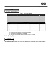
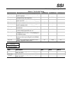
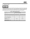
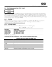
The information to be contained in the FRU device is shown in the following table.
Table 23: FRU Device Information
Area Type Description
Common Header As defined by the FRU document
Internal Use Area Not required, do not reserve
Chassis Info Area Not applicable, do not reserve
Board Info Area Not applicable, do not reserve
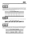
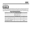
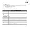
8.4.2.1 Product Info Area
As defined by the IPMI FRU document. Product information shall be defined as follows:
Table 24: FRU Device Product Information Area
Field Name Field Description
Manufacturer Name {Formal name of manufacturer}
Product Name {Manufacturer’s model number}
Product part/model
number
Customer part number
Product Version Customer current revision
Product Serial Number {Defined at time of manufacture}
Asset Tag {Not used, code is zero length byte}
FRU File ID {Not required}
PAD Bytes {Added as necessary to allow for 8-byte offset to next area}