


BIOS SETUP
30 MI935 User’s Manual
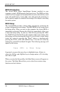
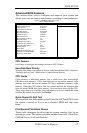
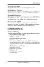
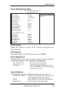
Advanced Chipset Features
This Setup menu controls the configuration of the chipset.
Phoenix - AwardBIOS CMOS Setup Utility
Advanced Chipset Features
DRAM Timing Selectable By SPD ITEM HELP
CAS Latency Time Auto Menu Level >
DRAM RAS# to CAS# Delay
DRAM RAS# Precharge
Precharge dealy (tRAS)
System Memory Frequency
System BIOS Cacheable
Memory Hole at 15M-16M
PCI Express Root Port Func
Auto
Auto
Auto
By SPD
Enabled
Disabled
Press Enter
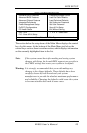
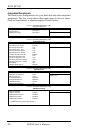
** VGA Setting **
PEG/On Chip VGA Control Auto
On-Chip Frame Buffer Size 8MB
DVMT Mode DVMT
DVMT/FIXED memory Size 128MB
SDVO Device Setting None
SDVO LVDS Protocol 1CH 18 bit
SDVO Panel 1024x768
Boot Display CRT+LVDS
TV Standard Off
Video Connector Automatic
TV Format Auto
DRAM Timing Selectable
This option refers to the method by which the DRAM timing is selected.
The default is By SPD.
CAS Latency Time
You can select CAS latency time in HCLKs of 3/3 or 4/4. The system
board designer should set the values in this field, depending on the
DRAM installed. Do not change the values in this field unless you
change specifications of the installed DRAM or the installed CPU. The
choices are 3, 4 and 5.
DRAM RAS# to CAS# Delay
This option allows you to insert a delay between the RAS (Row Address
Strobe) and CAS (Column Address Strobe) signals. This delay occurs
when the SDRAM is written to, read from or refreshed. Reducing the
delay improves the performance of the SDRAM.
DRAM RAS# Precharge
This option sets the number of cycles required for the RAS to
accumulate its charge before the SDRAM refreshes.