PD672X/30/32/33 — ZV Port Implementation
Application Note 11
7.0 ZV Port Implementation for Socket A and B
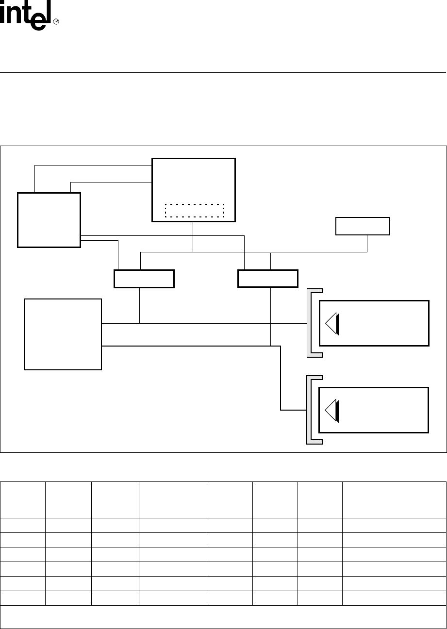
Figure 4 shows the ZV Port support for socket A and B. If using the GD7XXX, two of the GPO
pins can control the buffer output enables. Since there is only one V-Port, a ZV Port PC Card can
be inserted in either Socket A or Socket B.
Figure 4. ZV Port Implementation for Socket A and B
Table 1. PC Card, ZV Port, and PD6722 Pin Assignment (Sheet 1 of 2)
PC Card
Pin
Number
PC Card
Pin
I/O in PC
Card
Mode
ZV Port Pin
Name
I/O in ZV
Port Mode
PD6722S
ocket A
PD6722S
ocket B
Comments
8 A10 I HREF O 21 85 Horizontal sync to ZV Port
10 A11 I VSYNC O 25 89 Vertical sync to ZV Port
11 A9 I Y0 O 28 91 Video data to ZV Port
12 A8 I Y2 O 30 93 Video data to ZV Port
13 A13 I Y4 O 33 95 Video data to ZV Port
14 A14 I Y6 O 35 97 Video data to ZV Port
NOTE: ‘I’ indicates that the signal is an input to the PC Card; ‘O’ indicates that the signal is an output from the PC Card.
Controller ignores BVD2/SPKR#, IOIS16#, and INPACK# during ZV Port operation.
GD7XXX
V-PORT
ZV PORT PC CARD
AUDIO
PC CARD BUS A
ZV PORT PC CARD
BUFFER
BUFFER
GLUE LOGIC
2 NAND GATES
1 INVERTER
TVON
VPCNTL
OE
OE
R
P
Z
X
PC CARD BUS B
SOCKET A
SOCKET B
PD6722
PD6729
PD6730
PD6832
PD6833


