


PD672X/30/32/33 — ZV Port Implementation
Application Note 15
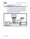
8.0 Layout Guidelines
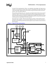
The VGA controller, the PC Card (PCMCIA) Controller, and the PC Card Sockets must be in close
proximity to one another. This requirement is particularly important when the PD6832 or PD6833
device is used along with the ZV Port for Card bus implementation. According to tests conducted
by PCMCIA ZV Port subcommittee, the stubs to the GD7548 device or any other VGA controller
must be no longer than two inches. As shown in Figure 4 on page 11, the stub length is the distance
between points P and R for PC Card bus A and between points X and Z for PC Card bus B. Vias
have already been included in this recommended stub length.
• Maximum total capacitive loading for each Card bus signal = 22 pF
• Maximum input capacitance of each host controller pin = 10 pF
• Maximum input capacitance of the buffer pin = 5 pF
A total of 7 pF remains for the PC Card connector-to-buffer input pin trace. A maximum trace
length of two inches satisfies CardBus requirements.
System designers must check the V
CC
bounce, ground bounce, and crosstalk on CardBus/ZV Port
prototypes to ensure that the effect is minimal. The CCLK signal on the CardBus must be thick
with sufficient gap from adjacent traces and series termination must be used. Guidelines for CCLK
signal are included in the latest PC Card specifications.
Note: Intel recommends that designers contact the PCMCIA organization for the latest revision of the ZV
Port standard.