


Chapter 4
Specifications
Typical for 25 °C unless otherwise specified.
Specifications in italic text are guaranteed by design.
The counter frequency sources and 3.3 V compatibility apply to hardware manufactured
at revision 3 and later
The clock input frequency sources and compatibility with a 3.3 V signaling environment that are listed in
this specification apply to hardware built at revision 3 and later.
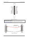
Digital input / output
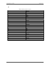
Table 4-1. Digital I/O specifications
Discrete, 5V/TTL compatible
Output: 74ACT273
Digital type
Input: 74LS373
Number of I/O 8 input, 8 output
Configuration 1 bank of 8 as output, 1 bank of 8 as strobed input
Input high voltage 2.0 V min, 7.0 V absolute max
Input low voltage 0.8 V max, –0.5 V absolute min
Output high voltage 3.94 volts min @ -24 mA (Vcc = 4.5 V)
Output low voltage 0.36 volts max @ 24 mA (Vcc = 4.5 V)
Data transfer Programmed I/O
Power-up / reset state Digital outputs reset to TTL low
Din strobe Active low latch enable input, internally pulled high through 10 KOhm resistor
Din strobe pulse width high/low 15 nS min
Data setup to Din strobe 5 nS min
Data hold from Din strobe 20 nS min
Interrupt
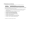
Table 4-2. Interrupt specifications
Number of user interrupts One
PCI Interrupt PCI INTA# - mapped to IRQn via PCI BIOS at boot-time
Interrupt enables
External: IRQ ENABLE, active low, disabled by default through internal
resistor to TTL high) and programmable through PCI9030-AA60PI; 0 =
disabled, 1 = enabled (default)
External: IRQ IN, polarity programmable through PCI9030-AA60PI;
1 = active high, 0 = active low (default).
Interrupt sources
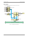
IRQ IN maps to PLX 9030 LINT1.
4-1