


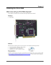
PCI-CTR05 User's Guide Introducing the PCI-CTR05
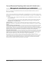
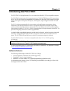
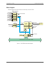
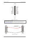
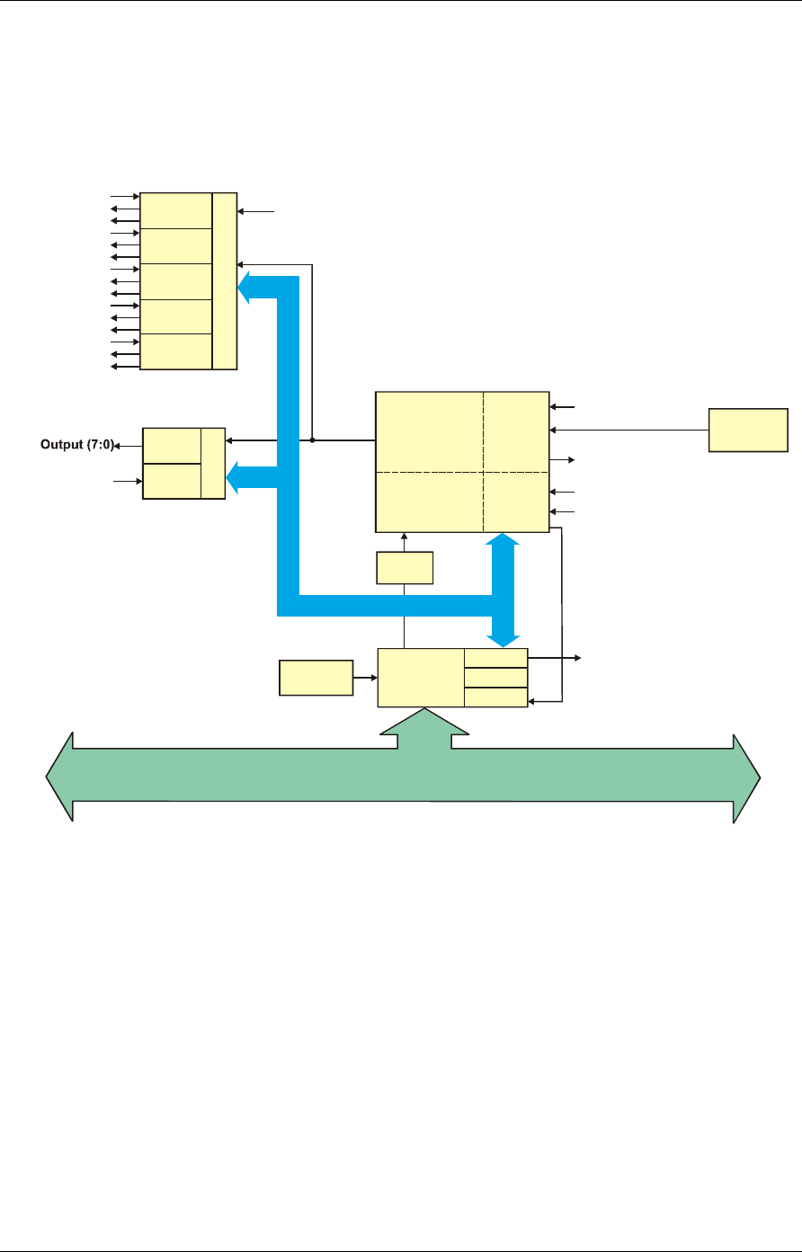
Block diagram
The block diagram shown here illustrates the functionality of the PCI-CTR05.
PCI
Controller
BADR1
Interrupt
Boot
EEPROM
Control
Registers
Clock
Divider
Decode/Status
Int
Ctl
Bus
Timing
Clock Select
1.0/1.67/3.3/5.0 MHz
EXT_INT_EN
EXT_INT
Controller FPGA and Logic
10
Oscillator
MHz
Local Bus
PCI Bus (5V/3.3V, Universal 32-Bit, 33 MHz)
Output
Port
Input
Port
Control
Input (7:0)
Digital I/O
Counter 0
Control
AMD9513 (equivalent)
16-bit counters
Counter 1
Counter 2
Counter 3
Counter 4
Clock Select
Control
Bus
Input Clock0
Gate0
Output Clock0
Input Clock1
Gate1
Output Clock1
Input Clock2
Gate2
Output Clock2
Input Clock3
Gate3
Output Clock3
Input Clock4
Gate4
Output Clock4
BADR2
1.0/1.67/3.3/5.0 MHz
Figure 1-1. PCI-CTR05 functional block diagram
1-2