


Chapter 3 Signal Connections
© National Instruments Corporation 3-17 DAQCard-700 User Manual
• Absolute maximum voltage input rating -0.5 to 5.0 V with respect to DGND
• MSM82C54 digital input specifications (referenced to DGND):
–V
IH
input logic high voltage 2.2 V minimum
–V
IL
input logic low voltage 0.8 V maximum
– Input load current ±10.0 µA maximum
• MSM82C54 digital output specifications (referenced to DGND):
–V
OH
output logic high voltage 3.0 V minimum
–V
OL
output logic low voltage 0.40 V maximum
–I
OH
output source current, at V
OH
2.5 mA maximum
–I
OL
output sink current, at V
OL
2.5 mA maximum
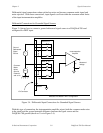
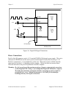
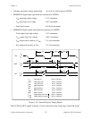
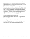
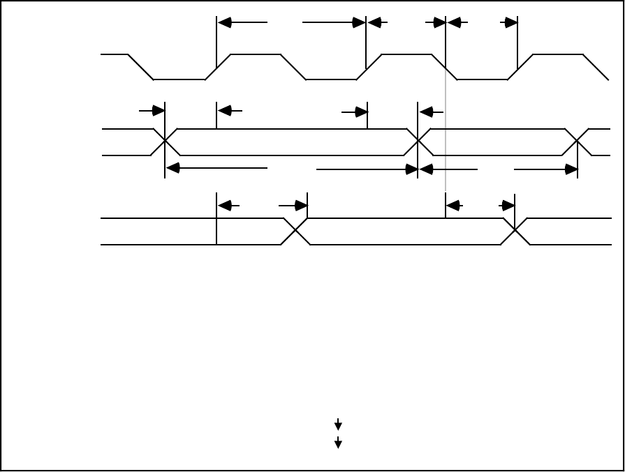
CLK
V
IH
V
IL
V
IH
V
IL
t
sc
t
pwh
t
gsu
t
gh
t
gwh
GATE
t
outg
OUT
V
OH
V
OL
t
pwl
t
gwl
t
outc
100 ns minimum
30 ns minimum
40 ns minimum
50 ns minimum
50 ns minimum
100 ns maximum
50 ns minimum
100 ns maximumt
outg
t
outc
t
gwh
t
gwl
t
gh
t
gsu
t
pwl
t
pwh
t
sc
clock period
clock high level
clock low level
gate setup time
gate hold time
gate high level
gate low level
output delay from clock
output delay from gate
50 ns minimum
Figure 3-10. General-Purpose Timing Signals
The GATE and OUT signals in Figure 3-10 are referenced to the rising edge of the CLK signal.