


Theory of Operation Chapter 4
DAQCard-700 User Manual 4-8 © National Instruments Corporation
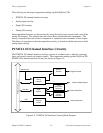
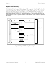
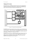
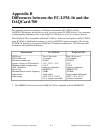
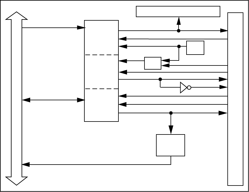
Timing I/O Circuitry
The DAQCard-700 uses an MSM82C54 counter/timer integrated circuit for data acquisition
timing and for general-purpose timing I/O functions. Three counters of the MSM82C54 are
available for general use, but one of them can be used internally for data acquisition timing.
Figure 4-5 shows a block diagram of both groups of timing I/O circuitry.
PCMCIA I/O Channel
OUT0
GATE0
CLK0
CLK1
GATE1
OUT1
CLK2
GATE2
OUT2
CTR RD/WR
8
/
Data
OUT0
GATE0
CLK1
GATE1
I/O Connector
1-MHz
Clock
Interrupt
Interface
A/D Conversion Logic
MSM82C54
Counter/Timer
Input
Mux
OUT1
OUT1*
CLK2
GATE2
OUT2
Figure 4-5. Timing I/O Circuitry Block Diagram
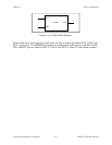
The MSM82C54 contains three independent 16-bit counter/timers and one 8-bit Mode Register.
As shown in Figure 4-5, counter 0 can be used for data acquisition timing, and counters 1 and 2
are free for general use. All three counter/timers can be programmed to operate in several useful
timing modes. The programming and operation of the MSM82C54 is presented in detail in the
optional DAQCard-700 Register-Level Programmer Manual.
The MSM82C54 for counter 0 uses a 1 MHz clock generated from the onboard oscillator. The
timebases for counters 1 and 2 can be supplied externally through the 50-pin I/O connector. In
addition, counter 1 can optionally use the same onboard 1 MHz clock that is used for data
acquisition timing, which facilitates synchronous operations. The 16-bit counters in the
MSM82C54 can be diagrammed as shown in Figure 4-6.