


Chapter 4 Connecting Signals
© National Instruments Corporation 4-13 NI 6115/6120 User Manual
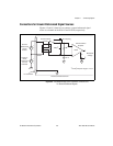
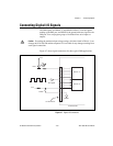
Like any amplifier, the common-mode rejection ratio (CMRR) of the PGIA
is limited at high frequency. This limitation has been compensated for in the
design of the NI 6115/6120 by using a common-mode choke on each
channel.
♦ NI 6115
The purpose of the 10 nF capacitance on the ACH<0..3>– connection of the
NI 6115 is to provide an impedance for this choke to work against at high
frequency, thus improving the high-frequency CMRR. Depending on your
application and the type of common noise at your source, further
common-noise rejection might be gained by placing a 0.1 µF ceramic
bypass capacitor between ACH– and ACH0GND.
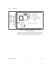
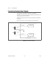
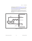
Working Voltage Range
The PGIA operates normally by amplifying signals of interest while
rejecting common-mode signals as long as the following three conditions
are met:
1. The common-mode voltage (V
cm
),
which is equivalent to subtracting
ACH<0..3>GND from ACH<0..3>– and which is shown in Figure 4-2,
must be less than ±2.5 V. This V
cm
is a constant for all range selections.
2. The signal voltage (V
s
), which is equivalent to subtracting
ACH<0..3>– from ACH<0..3>+ and which is shown in Figure 4-2,
must be less than or equal to the range selection of the given channel.
If V
s
is greater than the range selected, the signal clips and information
is lost.
3. The total working voltage of the positive input, which can be thought
of as (V
cm
+ V
s
) or simply as subtracting ACH<0..3>GND from
ACH<0..3>+, must be less than ±11 V for ranges ≤ ±10 V or less than
±42 V for ranges > ±10 V.
If any of these conditions are exceeded, current limiters limit the input
current to 20 mA maximum into any input until the fault condition is
removed.
Note All inputs are protected at up to ±42 V.