


Chapter 2 Connecting Signals
SCXI-1141/1142/1143 User Manual 2-6 ni.com
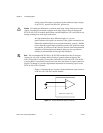
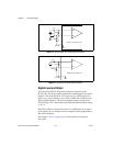
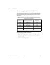
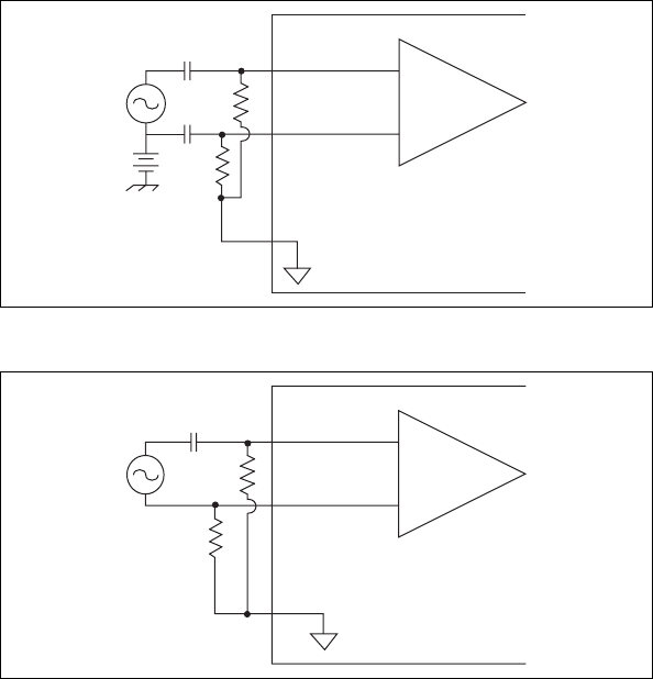
Figure 2-4. Ground Offset AC-Coupled Signal Connection
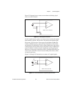
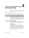
Figure 2-5. Floating AC-Coupled Signal Connection
Digital Input and Output
You can use the EXT CLK input pin on the front connector of the
SCXI-1141/1142/1143 module to control filter cutoff frequency for special
purposes. The clock should be a TTL-logic-level or CMOS-logic-level
square wave, with a frequency of less than 2.5 MHz that is 100 times the
desired cutoff frequency. The absolute maximum input voltage for the
EXT CLK pin is 5.5 V with respect to D GND; the minimum input voltage
is –0.5 V.
The OUT CLK pin on the front connector is a CMOS-logic-level output
clock, which you can configure to have a frequency that is proportional to
filter cutoff frequency.
See Chapter 4, Theory of Operation, for more details on using these
two signals.
1 µF
1 µF
1 MΩ
1
MΩ
A
SCXI-1141/1142/1143
A GND
IN–
IN+
1 µF
1 MΩ
A GND
SCXI-1141/1142/1143
A
100 kΩ
IN–
IN+