591
APPENDIX B DEVELOPMENT TOOLS
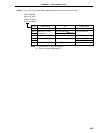
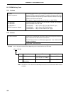
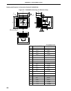
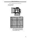
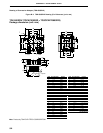
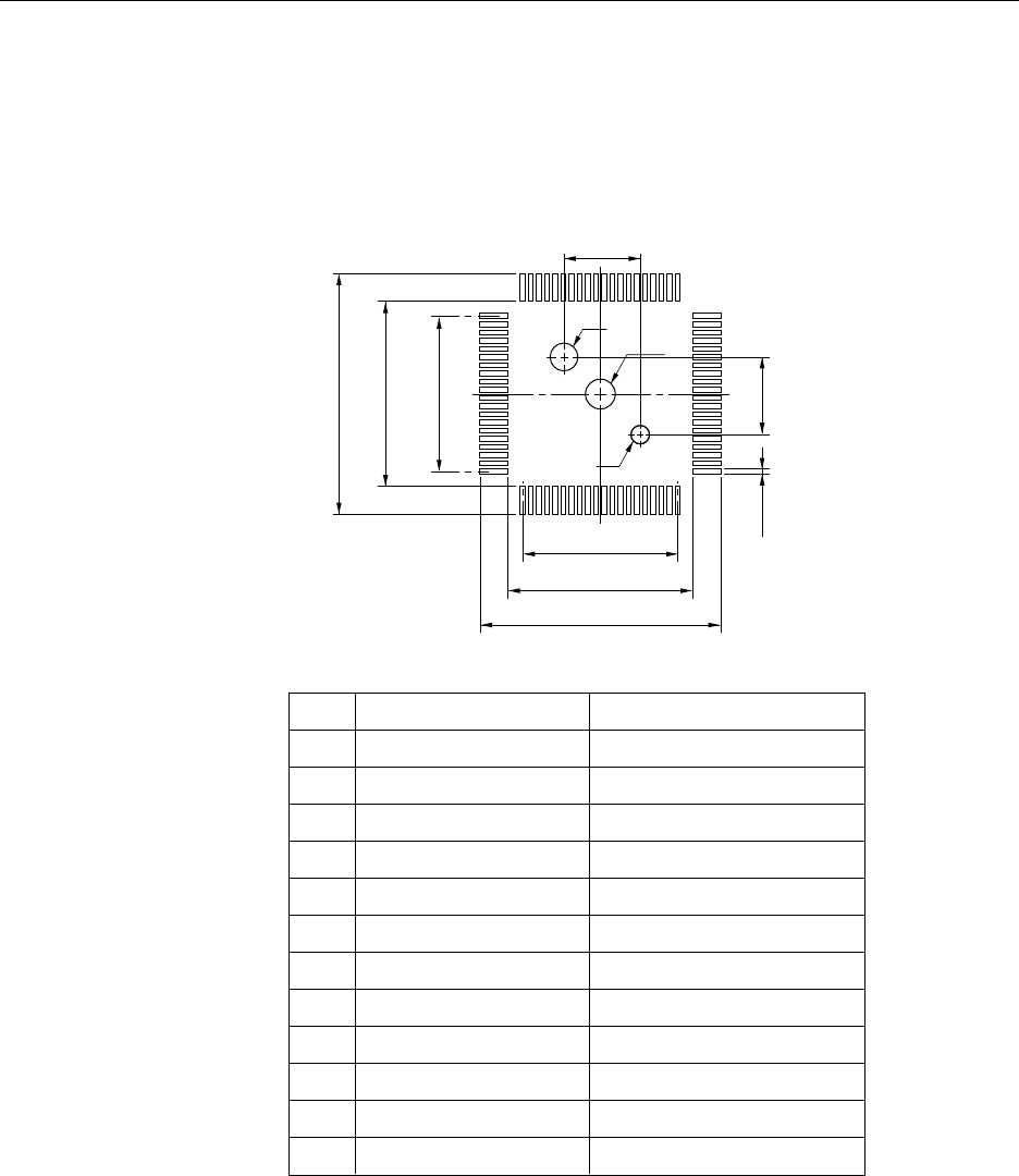
Figure B-3. EV-9200GC-80 Footprint (For Reference Only)
A
F
D
E
C
B
G
J
K
L
HI
0.026 × 0.748=0.486
0.026 × 0.748=0.486
EV-9200GC-80-P1E
ITEM MILLIMETERS INCHES
A
B
C
D
E
F
G
H
I
J
K
L
19.7
15.0
15.0
19.7
6.0
±
0.05
6.0
±
0.05
0.35
±
0.02
2.36
±
0.03
2.3
1.57
±
0.03
0.776
0.591
0.591
0.776
0.236
0.236
0.014
0.093
0.091
0.062
0.65
±
0.02 × 19=12.35
±
0.05
0.65
±
0.02 × 19=12.35
±
0.05
φ
φ
+0.001
–0.002
+0.003
–0.002
+0.001
–0.002
+0.003
–0.002
+0.003
–0.002
+0.003
–0.002
+0.001
–0.001
+0.001
–0.002
φ
+0.001
–0.002
φ
φ
Based on EV-9200GC-80
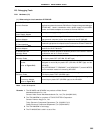
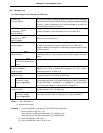
(2) Pad drawing (in mm)
Dimensions of mount pad for EV-9200 and that for
target device (QFP) may be different in some parts.
For the recommended mount pad dimensions for
QFP, refer to "SEMICONDUCTOR DEVICE MOUNTING
TECHNOLOGY MANUAL" (C10535E).
Caution
φ


