


- -9
5 MEMORY OPTIONS
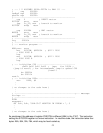
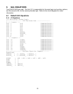
The RMB-167 memory decoding is accomplished by two 16V8-type GAL devices, U1 and U2.
Both devices are collectively responsible of selecting the options of determining the memory map.
An output of U1, AUX0 is an input to U2. Similarly, AUX1 connects the two devices. The signal
on AUX1 may flow in either direction, giving a wide range of possible ways to divide the
functionality between the two devices. A slide switch is also provided to allow switching between
alternate memory maps. The GAL inputs include RSTIN# and RSTOUT#, so that a memory map
swap upon completion of the reset process is possible, as explained in the Siemens Application
Notes. The RMB-167 decodes the address lines A13 to A17. Thus the memory map may be
constructed in blocks of 16K. For example, EPROM may occupy only the lower 16K of memory,
whereas RAM occupy the remaining addresses. The GAL equations for the default configuration
are given in Section 5.1.
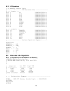
5.1 RAM Memory Options
Either 32K 62C256-type or 128K 681000-type static RAM chips may be used. Two chips are
needed, one for EVEN and the other for ODD addresses.
5.2 EPROM Memory Options
The RMB-167 has sockets to accommodate two 27C256-type 32K EPROMS. Two chips are
needed, one for EVEN and the other for ODD addresses. The EPROMS may be configured to
occupy low memory, high memory, or start at low memory and then relocate to high memory upon
initialization by appropriate jumper selections.
The SAB C167 may be programmed to insert wait cycles during external memory access.
However, in order to run the SAB C167 at its full potential of 40MHz, the RAMs should be rated at
70 nano seconds or faster, and the EPROMs should be rated at 85 nano seconds or faster.
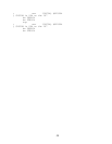
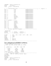
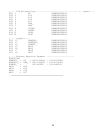
5.3 Alternate Memory Map with EPROM in Low Memory
The default RMB-167 memory map uses only the RAM chips. That is the range 0 to FFFFh is
decoded as RAM. The addresses are decoded by a GAL device. Alternate memory maps are
possible by changing the GAL programs. Moreover, several jumper inputs allow switching
between memory maps by changing jumper configurations. One possible implementation is given
below. Other memory maps are possible with different GAL equations.
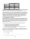
The jumpers marked CFG0 and CFG1 are used to switch between the memory maps as shown
below. In words, CFG0 determines the memory type for the lower 32K of memory, and CFG1, the
higher. Inserting a jumper selects EPROM. The GAL equations to achieve the alternate memory
maps are given in Section 5.2.