


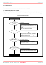

M30880T-EPB User’s Manual 4. Hardware Specifications
REJ10J0497-0100Z Rev.1.00 January 16, 2005
Page 88 of 100
IMPORTANT
Notes on EMEM Dialog Box:
Observe the following when setting up EMEM dialog box of the emulator debugger.
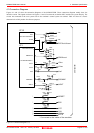
(1) Debug Monitor Bank Address
The default value of Debug Monitor Bank Address is "F0". To set single-chip mode, internal flash memory
is automatically allocated in F000h--FFFFh and F80000h--FFFFFFh.
The specified value becomes effective after restarting the system.
When "F0" is specified, 64 KB of area starting from F00000h are allocated for use by the debug monitor.
The 64 KB allocated for the debug monitor cannot be used.
The below areas cannot be set for the debug monitor.
1) MCU internal resources (ROM/RAM/SFR area)
2) Interrupt vector area
It is not possible to view or set the content of the specified area. Even on the memory window or in the
reverse assemble area of the program/source windows, the content of this area is not displayed correctly
though it can be displayed.
(2) Processor Mode
Set a single-chip mode for the target MCU.
To set single-chip mode, pin CNVSS used with MCU status must be "L". MCU status indicates pin level of
the user system.
(3) Emulation Memory Allocation
Because the available processor mode is the single-chip mode only, select the “No Use” in “Map”.
When single-chip mode is set as a processor mode, ROM area is automatically allocated to the internal
Flash ROM of an MCU.
MCU internal resources are automatically selected for SFR, RAM and ROM areas regardless of settings.
Emulator main unit's memory is automatically selected as a reset vector area regardless of settings.
Notes on Watchdog Function:
When using the watchdog function, select the check box of "Debug the program using the Watchdog Timer" in
the MCU tab of the Init dialog box. When not using the watchdog function, clear the check box.
If the reset circuit of the user system has a watchdog timer, disable it when using the emulator.