


( 7 / 12 )
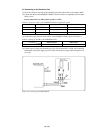
No.
SW1
SW2
SW3
Name
PORT/XCIN
VREF
CNVss
Function
Allows you to choose whether to supply the sub-clock
signals (32.768 kHz) to the MCU's XCIN pin (pin 16).
To use pin P21/XCIN as an I/O port, choose the PORT
side.
To use the sub-clock signals, choose the XCIN side.
Allows you to choose whether to apply Vcc or some
other source to the MCU's VREF pin (pin 2). In the
case of the latter, choose the J1-2 side, and apply a
voltage within a prescribed range to the J1-2.
Allows you to choose which to connect, Vcc or Vss, to
the MCU's CNVss (pin 15).
Factory-setting
PORT
Vcc
Vss
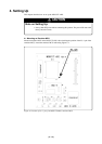
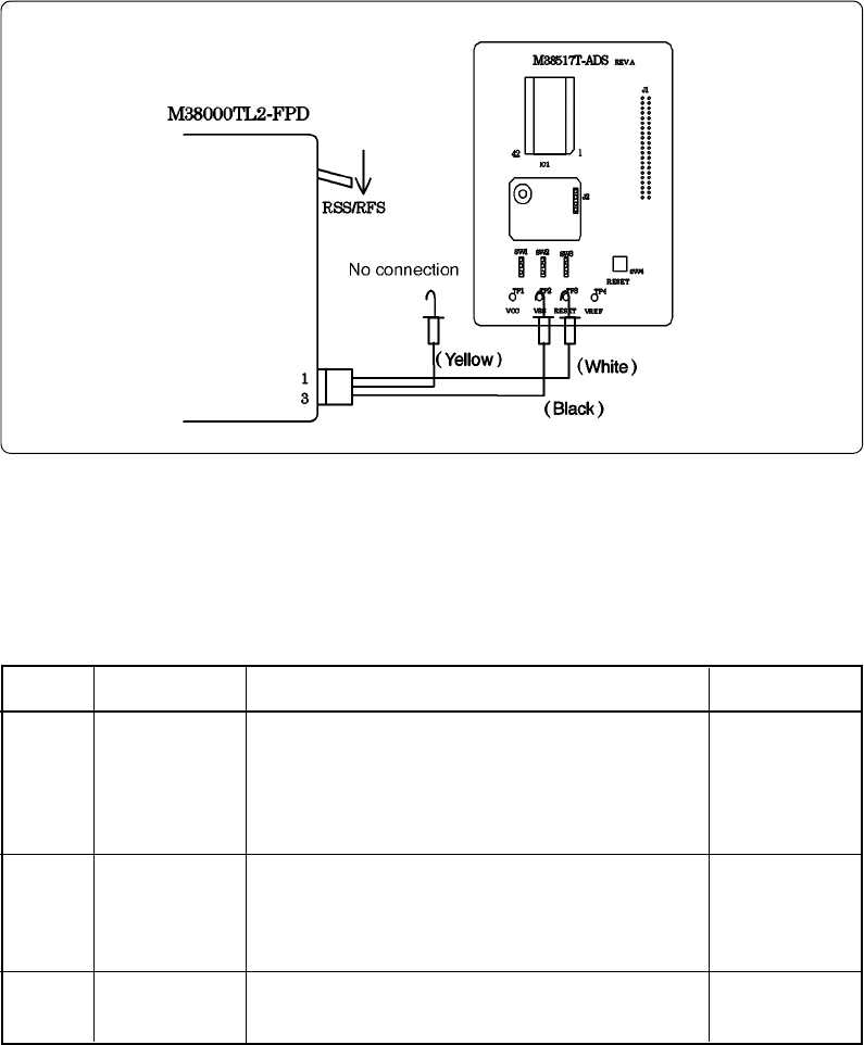
Figure 4.3 Connecting the M38517RSS
4.3 Setting the Switches
Set the switches SW1 to SW3 according to your applications. Table 4.3 describes the functions of
the switches SW1 to SW3.
Table 4.3 Functions of the switches SW1, SW2 and SW3