


Operational Specifications
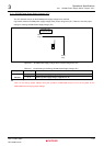
3.1.7 Extension Connector (J14)
Rev.1.0 Feb 6, 2007 3-16
REJ10J0916-0100
3
3.1.7 Extension Connector (J14)
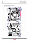
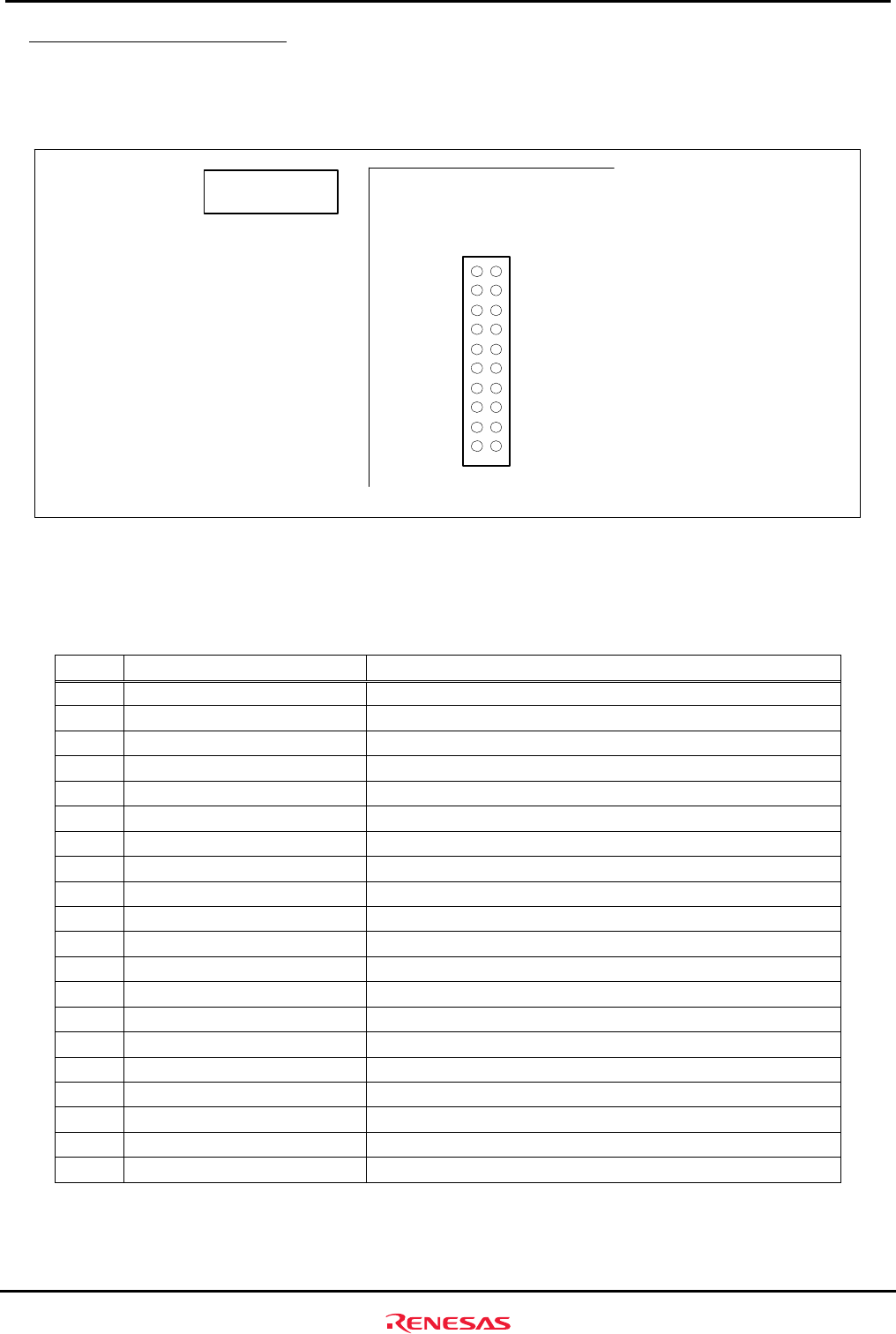
Extension connector(J14) connects the pins necessary for writing a on-chip flash memory of SH7086.
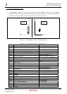
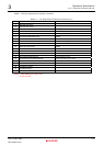
Figure 3.1.9 lists pin assignments of the extension connectors.
Board Edge
19
20
1
2
J14
Top View of the
Component Side
Board Edge
Figure 3.1.9 Pin Assignments of the Extension Connector (J14)
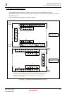
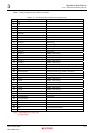
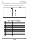
Table 3.1.14 lists pin assignments of the extension connector (J14).
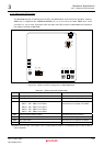
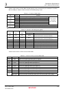
Table 3.1.14 Pin Assignments of the Extension Connector (J14)
Pin Signal Name Other Connection
1 RES
________
-
2 GND -
3 FWE FWE pin select jumper (JP2)
4 GND -
5 MD0 DIP switch for system setting (SW4-3)
6 GND -
7 MD1 DIP switch for system setting (SW4-2)
8 GND -
9 NC -
10 GND -
11 NC -
12 GND -
13 NC -
14 GND -
15 PA4/A23/TXD1 Serial port connector (J3)
16 GND -
17 PA3/A24/RXD1 Serial port connector (J3)
*
18 VCC -
19 NC -
20 VCC -
Note *: It is connected to the output pin of RS-232C driver.