


M61323SP/FP
REJ03F0201-0201 Rev.2.01 Mar 31, 2008
Page 17 of 19
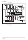
Note How to Use This IC (M61323SP)
1. R, G, B input signal is 0.7 V
P-P
of standard video signal.
2. H, V input is 5.0 V TTL type.
3. Input signal with sufficient low impedance to input terminal.
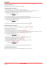
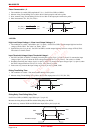
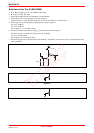
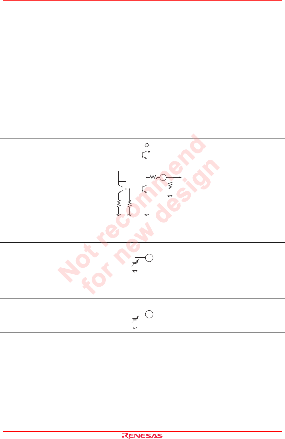
4. The terminal of R, G, B output pin are shown as figure 1.
When resistance is connected between the pin 31 (28, 25) and GND, I
CC
will be increase.
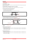
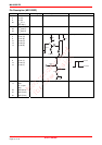
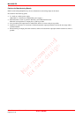
5. Switch (pin 13) can be changed by supplying some voltage as figure 2.
0 to 0.5 V: INPUT1
2.5 to 5 V: INPUT2
Do not apply V
CC
or more DC voltage.
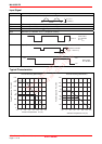
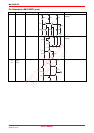
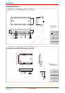
6. Power save mode is provided for saving I
CC
less than about 10 mA as figure 3.
0 to 0.5 V: Power save mode (H.V-SW, Sync-Sep., G-Buffer)
2.5 to 5 V: Normal mode
Do not apply 5 V or more DC voltage
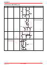
7. When not use the Sync-separation circuit built in this IC, capacitance of several tens of pF is required between the
pin 22 and GND.
R
I < 5 mA
5 V
50 Ω
600 Ω
Figure 1
13
Figure 2
11
Figure 3