


SH7145F
Asynchronous Serial Data Transmission/Reception
REJ06B0357-0100O/Rev.1.00 March 2004 Page 3 of 17
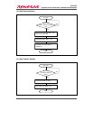
2 Functions Used
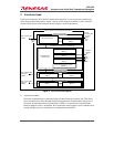
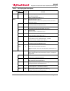
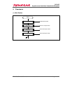
In this task example the SCI (Serial Communication Interface) is used to perform asynchronous
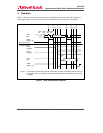
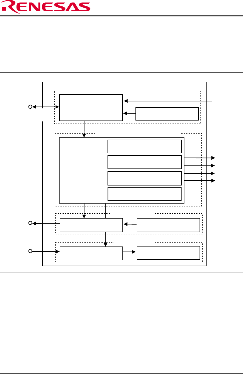
serial data transmission/reception. Figure 2 shows a block diagram of channel 1 (ch1) of the SCI
module. The functions of the elements shown in figure 2 are described below.
TEI_1
TXI_1
RXI_1
ERI_1
SCI1 clock I/O pin
(SCK1)
SCI1 transmit data
output pin
(TXD1)
SCI1 receive data
input pin
(RXD1)
SCI0 synchronous serial transfer function block
Baud rate generator
Bit rate register 1
(BRR_1)
Clock
Transmit/receive operation control settings
Transfer rate generator
Serial mode register 1
(SMR_1)
Serial control register 1
(SCR_1)
Serial status register 1
(SSR_1)
Serial direction control register 1
(SDCR_1)
Transmit/receive
control circuit
Interrupt
requests
Transmit data control
Transmit shift register 1
(TSR_1)
Transmit data register 1
(TDR_1)
Receive data control
Receive shift register 1
(RSR_1)
Receive data register 1
(RDR_1)
External
clock
Pφ/128
Pφ/32
Pφ/8
Pφ1
On-chip
peripheral cloc
k
Figure 2 SCI (ch1) Block Diagram
• Asynchronous Mode
Serial data communication is performed using synchronization by character unit. This allows
serial communication with a standard dedicated asynchronous communication chip such as a
Universal Asynchronous Receiver/Transmitter (UART) or Asynchronous Communication
Interface Adapter (ACIA). In addition, the asynchronous mode supports serial communication
among multiple processors (multiprocessor communication function).