


SH7145F
Asynchronous Serial Data Transmission/Reception
REJ06B0357-0100O/Rev.1.00 March 2004 Page 9 of 17
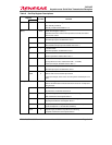
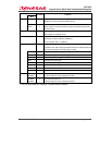
Table 6 On-Chip Register Descriptions
Register
Bit
Set Value Function
MSTCR1 MSTP17 0 Module standby control register 1
SCI1 standby control bit
Standby cancelled when MSTP17 = 0
SCR_1 H'70 Serial control register 1 (SCI_1)
Transmit and receive control, interrupt control, transmit and receive
clock source control
TIE 0 Transmit interrupt enable
TXI interrupt requests enabled when set to 1
RIE 1 Receive interrupt enable
RXI and ERI interrupt requests enabled when set to 1
TE 1 Transmit enable
Transmit operations enabled when set to 1
RE 1 Receive enable
Receive operations enabled when set to 1
MPIE 0 Multiprocessor interrupt enable
(In asynchronous mode, enabled when MP = 1 in SMR)
In the task example, disabled because MP = 0
TEIE 0 Transmit end interrupt enable
TEI interrupt requests enabled when set to 1
CKE1
CKE2
0
0
Clock enable 1, 0
Selects clock source and SCK pin function
In the task example, clock source is on-chip clock and SCK pin is not
used
SMR_1 H'00 Serial mode register 1
Selects communication format and the clock source for on-chip baud
rate generator
C/A 0 Communication mode
Asynchronous mode when cleared to 0
CHR 0 Character length (enabled in asynchronous mode only)
8-bit transmission and reception when 0
PE 0 Parity enable (enabled in asynchronous mode only)
No-parity transmission and reception when 0
O/E 0 Parity mode (enabled in asynchronous mode when PE = 1)
(In this example PE = 0 and this bit is disabled)
STOP 0 Stop bit length (enabled in asynchronous mode only)
1-stop-bit transmission and reception when 0