


October 2009
General Information DDR3 SDRAM
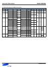
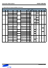
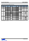
3 : DIMM
4 : SODIMM
Z FBGA(Lead-free)
H FBGA(Lead-free & Halogen-free)
J FBGA(Lead-free, DDP)
M FBGA(Lead-free & Halogen-free, DDP)
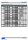
32
: 32M 33 : 32M (for 128Mb/512Mb)
64 : 64M 65 : 64M (for 128Mb/512Mb)
28 : 128M 29 : 128M (for 128Mb/512Mb)
56 : 256M 57 : 256M (for 512Mb/2Gb)
51 : 512M 52 : 512M (for 512Mb/2Gb)
1G : 1G 1K : 1G (for 2Gb)
2G : 2G 2K : 2G (for 2Gb)
M 1st Gen. A 2nd Gen.
B 3rd Gen. C 4th Gen.
D 5th Gen. E 6th Gen.
F : 7th Gen. G 8th Gen.
0 : None
2 : 2nd Rev.
4 : 4th Rev.
B : DDR3 SDRAM (1.5V VDD)
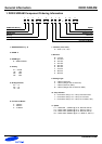
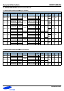
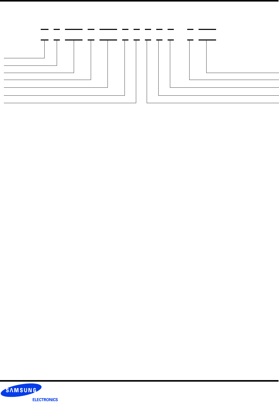
1. Memory Module : M
2. DIMM Type
3. Data Bits
4. DRAM Component Type
5. Depth
12. Speed
11. Temp & Power
10. PCB Revision
9. Package
8. Component Revision
7 : 8Banks & SSTL-1.5V
6. # of Banks in comp. & Interface
3. DDR3 SDRAM Module Ordering Information
:
:
:
:
:
:
:
:
:
:
:
1 : 1st Rev.
3 : 3rd Rev.
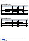
S : Reduced Layer
C
Y
: Commercial Temp.( 0°C ~ 85°C) & Normal Power
: Commercial Temp.( 0°C ~ 85°C) & Low VDD(1.35V)
Note: PC3-6400(DDR3-800),PC3-8500(DDR3-1066),
PC3-10600(DDR3-1333), PC3-12800(DDR3-1600)
PCB Revision
Component Revision
# of Banks in Comp. & Interface
Depth
DRAM Component Type
Data bits
DIMM Type
Memory Module
Package
Temp & Power
Speed
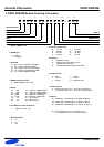
M X X X B X X X X X X X - X X X
1 2 3 4 5 6 7 8 9 10 11 12
Bit Organization
0 : x 4
3 : x 8
4 : x16
7. Bit Organization
: DDR3-800 (400MHz @ CL=6, tRCD=6, tRP=6)
: DDR3-1066 (533MHz @ CL=7, tRCD=7, tRP=7)
: DDR3-1333 (667MHz @ CL=9, tRCD=9, tRP=9)
: DDR3-1600 (800MHz @ CL=11, tRCD=11, tRP=11)
F7
F8
H9
K0
71
: x64 204pin Unbuffered SODIMM
78 : x64 240pin Unbuffered DIMM
91 : x72 240pin ECC unbuffered DIMM
92 : x72 240pin VLP Registered DIMM
93 : x72 240pin Registered DIMM