


Spinpoint M8U-Internal Product Manual REV 3.4
42
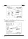
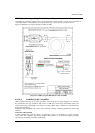
INSTALLATION
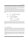
The magnitude of the current source and the value of the termination resistors are controlled to specified
tolerances, and together they determine the actual voltage drive levels. The DC resistance from D+ or D- to
the device ground is required to be 45Ω ±10% when measured without a load, and the differential output
voltage measured across the lines (in either the J or K state) must be ±400 mV ±10% when D+ and D- are
terminated with precision 45Ω resistors to ground.
The differential voltage developed across the lines is used for three purposes:
A differential receiver at the receiving end of the cable receives the differential data signal. A differential
envelope detector at the receiving end of the cable determines when the link is in the Squelch state. A receiver
uses squelch detection as indication that the signal at its connector is not valid.
In the case of a downstream facing hub transceiver, a differential envelope detector monitors whether the
signal at its connector is in the high-speed state. A downstream facing transceiver operating in high-speed
mode is required to test for this state at a particular point in time when it is transmitting a SOF packet. This is
used to detect device disconnection. In the absence of the far end terminations, the differential voltage will
nominally double (as compared to when a high-speed device is present) when a high-speed J or K are
continuously driven for a period exceeding the round-trip delay for the cable and
board-traces between the
two transceivers.
USB 2.0 requires that a downstream facing transceiver must be able to operate in low-speed, full-speed, and
high-speed signaling modes. An upstream facing high-speed capable transceiver must not operate in low- speed
signaling mode, but must be able to operate in full-speed signaling mode. Therefore, a 1.5 k Ωpu l l-up on the
D line is not allowed for a high-speed capable device, since a high-speed capable transceiver must never signal
low-speed operation to the hub port to which it is attached.
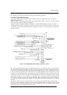
6.2.2.3 High-speed (480Mb/s) Driver Characteristics
A high-speed USB connection is made through a shielded, twisted pair cable with a differential characteristic
impedance (Z
0) of 90Ω ±15%, a common mode impedance (ZCM) of 30Ω ±30%, and a maximum one-way
delay of 26 ns (T
FSCBL). The D+ and D- circuit board traces which run between a transceiver and its associated
connector should also have a nominal differential impedance of 90Ω, and together they may add an additional
4 ns of delay between the transceivers. The differential output impedance of a high-speed capable driver is
required to be 90Ω ±10%.
When either the D+ or D- lines are driven high, VHSOH (the high-speed mode high-level output voltage driven
on a data line with a precision 45Ω load to GND) must be 400 mV ±10%. On a line which is not driven, either
because the transceiver is not transmitting or because the opposite line is being driven high, V
HSOL (the high
speed mode low-level output voltage driven on a data line with a 45Ω load to GND) must be 0 V ± 10mV.
Note: Unless indicated otherwise, all voltage measurements are to be made with respect to the local
circuit ground.
Note: This specification requires that a high-speed capable transceiver operating in full-speed or
low-speed mode must have a driver impedance (ZHSDRV) of 45Ω ±10%.
It is recommended that the driver impedances be matched to within 5Ω within a transceiver. For upstream
facing transceivers which do not support high- speed mode, the driver output impedance (Z
DRV) must fall
within the range of 28Ω to 44Ω.
On downstream facing ports, R
PD resistors (15 kΩ ±5%) must be connected
from D+ and D- to ground.
When a high-speed capable transceiver transitions to high-speed mode, the high-
speed idle state is achieved by driving SE0 with the low-/full-speed drivers at each end of the link (so as to
provide the required terminations), and by disconnecting the D+ pull-up resist
or in the upstream facing
transceiver. In the preferred embodiment, a transceiver activates its high-speed current driver only when
transmitting high speed signals. This is a potential design challenge, however, since the signal amplitude and
timing specifications must be met even on the first symbol within a packet. As a less efficient alternative, a
transceiver may cause its high-speed current source to be continually active while in high-speed mode. When
the transceiver is not transmitting, the current may be directed into the device ground rather than through the
current steering switch which is used for da
ta signaling. In CMOS implementations, the driver impedance will
typically be realized by the combination of the driver’s intrinsic output impedance and R
S. To optimally
control Z
HSDRV and to minimize parasitics, it is preferred the driver impedance be minimized (under 5Ω) and
the balance of the 45Ω should be contributed by the R
S component.