


Si53xx-RM
164 Rev. 0.5
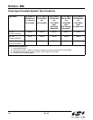
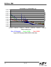
APPENDIX H—JITTER ATTENUATION AND LOOP BW
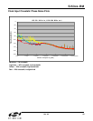
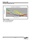
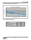
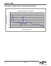
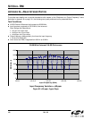
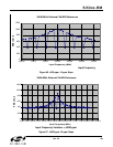
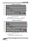
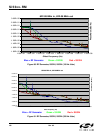
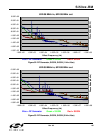
The following illustrates the effects of different loop BW values on the jitter attenuation of the Any-Frequency
devices. The jitter consists of sine wave modulation at varying frequencies. The RMS jitter values of the modulated
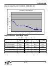
sine wave input is compared to the output jitter of an Si5326 and an Si5324. For reference, the top entry in the
table lists the jitter without any modulation. For each entry in the table, the corresponding phase noise plots are
presented.
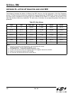
Table 82. Jitter Values
Fmod Fdev Jitter Start RF Gen Si5326 Si5324
0 0 500 Hz 1.18 ps 283 fs 281 fs
50 Hz 50 Hz 10 Hz 181 ps 169 ps 10.6 ps
100 Hz 100 Hz 50 Hz 177 ps 136 ps 2.04 ps
500 Hz 500 Hz 100 Hz 175 ps 18.6 ps 295 fs
1 kHz 1 kHz 500 Hz 184 ps 4.28 ps 292 fs
5kHz 5kHz 500Hz 138ps 297fs 302fs
10kHz 10kHz 500Hz 139ps 302fs 304fs
Notes:
1. All phase noise plots are with 622.08 MHz input and 622.08 MHz output.
Si5326 bandwidth = 120 Hz; Si5324 bandwidth = 7 Hz.
2. FM modulation at F = Fmod with modulation amplitude = Fdev.
3. Jit start is the start of the brick wall integration band. All integration bands end at 50 MHz.
4. Phase noise measured by Agilent model E5052B.
5. RF Generator was Rohde and Schwarz model SML03.