


Si53xx-RM
Rev. 0.5 171
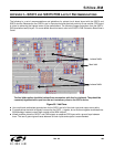
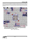
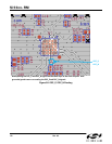
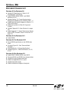
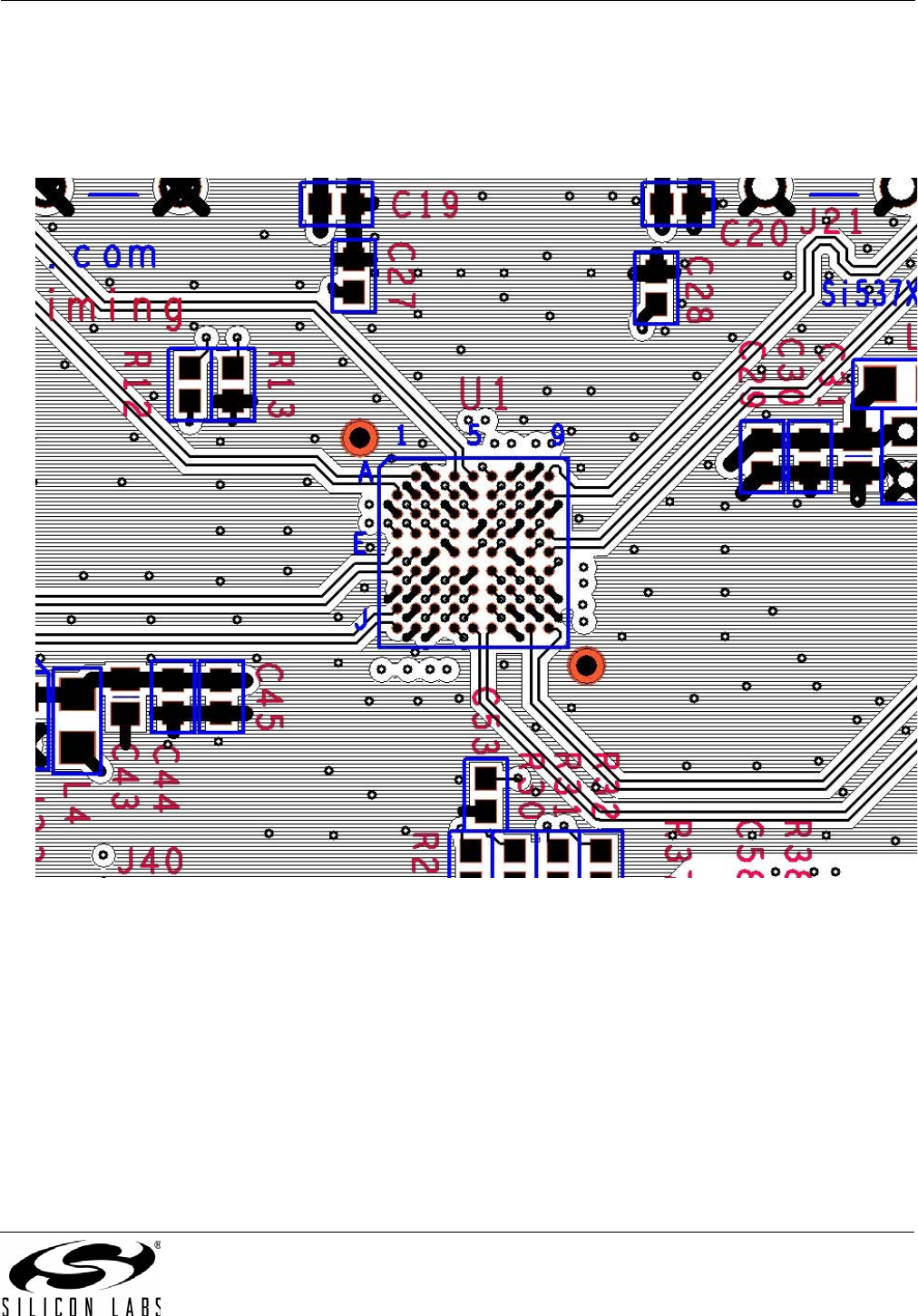
The following is a set of recommendations and guidelines for printed circuit board layout with the Si5374 and
Si5374 devices. Because the four DSPLLs are in close physical and electrical proximity to one another, PCB layout
is critical to achieving the highest levels of jitter performance. The following images were taken from the Si537x-
EVB (evaluation board) layout. For more details about this board, please refer to the Si537x-EVB Evaluation Board
User's Guide.
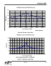
Figure 97. Output Clock Routing
As much as is possible, do not route clock input and output signals
underneath the BGA package. The clock output signals should go
directly outwards from the BGA footprint.