


Si53xx-RM
Rev. 0.5 85
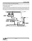
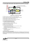
7.5. Si5319, Si5324, Si5326, Si5327, Si5368, Si5369, Si5374 and Si5375 Free Run Mode
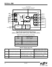
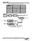
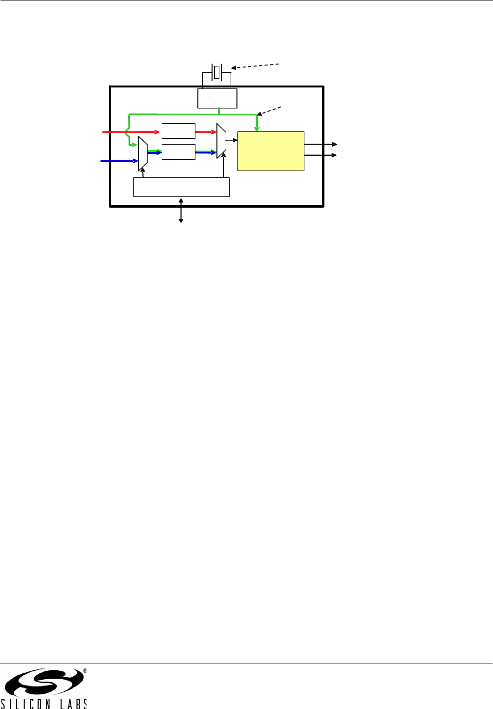
Figure 29. Free Run Mode Block Diagram
CKIN2 has an extra mux with a path to the crystal oscillator output.
When in Free Run mode, CKIN2 is sacrificed (Si5326, Si5368, Si5369, Si5374).
Switching between the crystal oscillator and CLKIN1 is hitless.
Either a crystal or an external oscillator can be used.
External oscillator connection can be either single ended or differential.
All other features and specifications remain the same.
7.5.1. Free Run Mode Programming Procedure
Using DSPLLsim, determine the frequency plan:
Write to the internal dividers, including N31 and N32.
Enable Free Run Mode (the mux select line), FREE_RUN.
Select CKIN1 as the higher priority clock.
Establish revertive and autoselect modes.
Once properly programmed, the part will:
Initially lock to either the XA/XB (OSC_P and OSC_N for the Si5374/75) or to CKIN1.
Automatically select CKIN1, if it is available.
Automatically and hitlessly switch to XA/XB if CKIN1 fails.
Automatically and hitlessly switch back to CKIN1 when it subsequently returns.
For the Si5319:
Clock selection is manual using an input pin.
Clock switching is not hitless.
CKIN2 is not available.
7.5.2. Clock Control Logic in Free Run Mode
Noting that the mux that selects CKIN2 versus the XA/XB oscillator is located before the clock selection and control
logic, when in Free Run mode operation, all such logic will be driven by the XA/XB oscillator, not the CKIN2 pins.
For example, when in Free Run mode, the CK2B pin will reflect the status of the XA/XB oscillator and not the status
of the CKIN2 pins.
Crystal or an external oscillator
(external oscillator only for the Si5374/75)
Si5319,
Si5324,
Si5326,
Si5327,
Si5368,
Si5369,
Si5374,
Si5375
CKOUT1
CKOUT2
Xtal osc
DSPLL
Core
CKIN1
I
2
C/SPI
CKIN2
Control
XA-XB
N31
N31
N32
N32
XAXB