


Si53xx-RM
96 Rev. 0.5
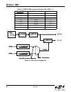
7.10. PLL Bypass Mode (Si5319, Si5324, Si5325, Si5326, Si5327, Si5367, Si5368, Si5369,
Si5374, Si5375)
The device supports a PLL bypass mode in which the selected input clock is fed directly to the output buffers,
bypassing the DSPLL. In PLL bypass mode, the input and output clocks will be at the same frequency. PLL bypass
mode is useful in a laboratory environment to measure system performance with and without the jitter attenuation
provided by the DSPLL. The BYPASS_REG bit controls enabling/disabling PLL bypass mode.
Before going into bypass mode, it is recommended that the part enter Digital Hold by setting DHOLD. Internally, the
bypass path is implemented with high-speed differential signaling for low jitter. Note that the CMOS output format
does not support bypass mode.
7.11. Alarms (Si5319, Si5324, Si5325, Si5326, Si5327, Si5367, Si5368, Si5369, Si5374,
Si5375)
Summary alarms are available to indicate the overall status of the input signals and frame alignment (Si5368 only).
Alarm outputs stay high until all the alarm conditions for that alarm output are cleared. The Register VALTIME
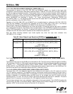
controls how long a valid signal is re-applied before an alarm clears. Table 48 shows the available settings. Note
that only for VALTIME[1:0] = 00, hitless switching is not possible.
7.11.1. Loss-of-Signal Alarms (Si5319, Si5324, Si5325, Si5326, Si5327, Si5367, Si5368, Si5369, Si5374,
Si5375)
The device has loss-of-signal circuitry that continuously monitors CKINn for missing pulses. The LOS circuitry
generates an internal LOSn_INT output signal that is processed with other alarms to generate CnB and
ALARMOUT.
An LOS condition on CKIN1 causes the internal LOS1_INT alarm become active. Similarly, an LOS condition on
CKINn causes the LOSn_INT alarm become active. Once a LOSn_INT alarm is asserted on one of the input
clocks, it remains asserted until that input clock is validated over a designated time period. If another error
condition on the same input clock is detected during the validation time then the alarm remains asserted and the
validation time starts over.
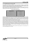
7.11.1.1. Narrowband LOS Algorithms (Si5319, Si5324, Si5326, Si5327, Si5368, Si5369, Si5374, Si5375)
There are three options for LOS: LOS, LOS_A, and no LOS, which are selected using the LOSn_EN registers. The
values for the LOSn_EN registers are given in Table 49.
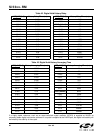
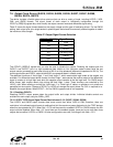
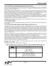
Table 48. Loss-of-Signal Validation Times
VALTIME[1:0] Clock Validation Time
00 2 ms
(hitless switching not available)
01 100 ms
10 200 ms
11 13 s
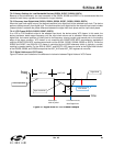
Table 49. Loss-of-Signal Registers
LOSn_EN[1:0] LOS Selection
00 Disable all LOS monitoring
01 Reserved
10 LOS_A enabled
11 LOS enabled