


Ultra Fast USB 2.0 Multi-Format Flash Media Controller/USB Hub Combo
SMSC USB2640/USB2641 21 Revision 2.0 (10-03-08)
DATASHEET
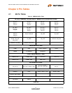
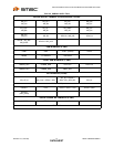
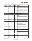
SPI Clock SPI_CLK /
GPIO4 /
SCL
9 I/O12 SPI_CLK: This is the SPI clock out to the serial
ROM. See Section 6.4, "ROM BOOT Sequence"
for diagram and usage instructions.
When the SPI interface is disabled, by setting the
SPI_DISABLE bit in the UTIL_CONFIG1 register,
this pin becomes GPIO4.
During reset, this pin must be driven low.
GPIO: This pin may be used either as input, edge
sensitive interrupt input, or output.
SCL: When configured, this is the I
2
C EEPROM
clock pin.
SPI Data Out SPI_DO /
GPIO5 / SDA /
SPI_SPD_SEL
10 I/O12 SPI_DO: This is the data out for the SPI port. See
Section 6.4, "ROM BOOT Sequence" for diagram
and usage instructions.
When the SPI interface is disabled, by setting the
SPI_DISABLE bit in the UTIL_CONFIG1 register,
this pin becomes GPIO5.
GPIO: This pin may be used either as input, edge
sensitive interrupt input, or output.
SDA: This pin is the data pin when the device is
connected to the optional I
2
C EEPROM.
SPI_SPD_SEL: This pin is used to pick the speed
of the SPI interface. During nRESET assertion,
this pin will be tri-stated with the weak pull-down
resistor enabled. When nRESET is negated, the
value on the pin will be internally latched, and the
pin will revert to SPI_DO functionality, the internal
pull-down will be disabled.
0 = 30 MHz
1 = 60 MHz
The firmware can see the state of this bit in the
SPI_CTL register.
Note:
If the latched value is '1', then the pin is tri-stated
when the chip is in the suspend state.
If the latched value is '0', then the pin is driven low
during a suspend state.
SPI Data In SPI_DI 11 I/O12PD This is the data in to the controller from the ROM.
This pin must have a weak internal pull-down
applied at all times to prevent floating.
Table 6.1 USB2640/USB2641 Pin Descriptions (continued)
NAME SYMBOL
48-PIN
QFN
BUFFER
TYPE DESCRIPTION