


Ultra Fast USB 2.0 Multi-Format Flash Media Controller/USB Hub Combo
Revision 2.0 (10-03-08) 22 SMSC USB2640/USB2641
DATASHEET
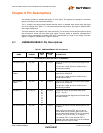
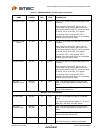
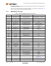
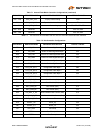
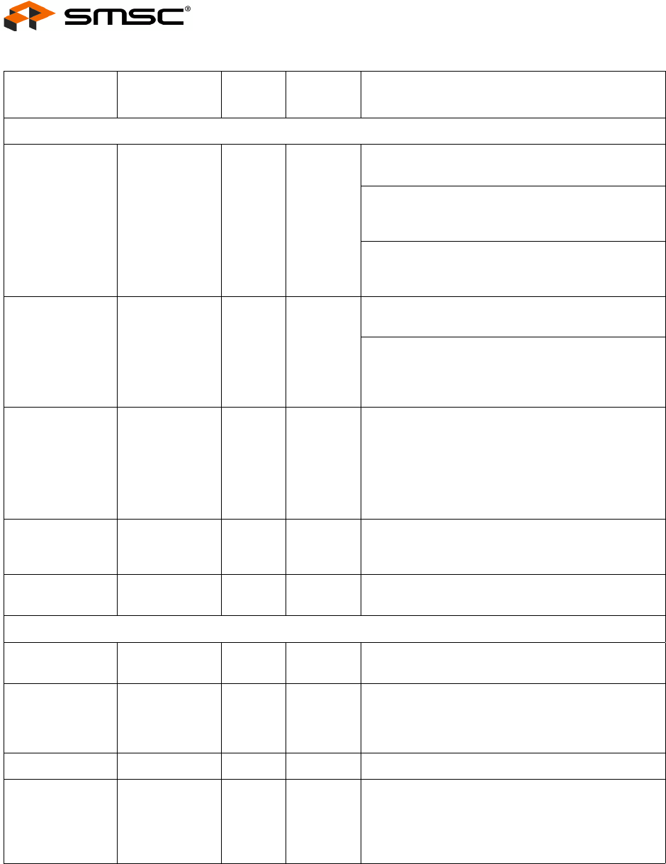
MISC
General Purpose
I/O
GPIO1 /
LED1 /
TXD
37 I/O12 GPIO: This pin may be used either as input, edge
sensitive interrupt input, or output.
LED: In addition, as an output, the GPIO1 can be
used as output controlled by the LED1_GPIO1
register.
TXD: The signal can be used as input to the TxD
of UART in the device when the TXD_SEL bit in
UTIL_CONFIG1 register is cleared to "0".
General Purpose
I/O
GPIO2 / RXD 36 I/O12 GPIO: This pin may be used either as input, edge
sensitive interrupt input, or output.
RXD: In addition to the above, the signal can be
used as input to the RXD of UART in the device
when the RXD_SEL bit in UTIL_CONFIG1 register
is cleared to "0".
General Purpose
I/O
GPIO10
(CRD_PWR)
35 I/O200 These pins may be used either as input, edge
sensitive interrupt input, or output. It is a
requirement that this is the only FET used to
power xD devices. Failure to do this will violate xD
voltage specification on xD device pins.
Card power drive: 3.3V (100 mA or 200 mA)
RESET input nRESET 38 IS This active low signal is used by the system to
reset the chip. The active low pulse should be at
least 1 μs wide.
TEST Input TEST 40 I This signal is used for testing the chip. If the test
function is not used, tie this pin low externally.
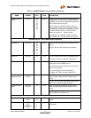
DIGITAL / POWER / GROUND
1.8V Digital Core
Power Bypass
VDD18 15 +1.8V Core power bypass. This requires an
external bypass capacitor of 1.0 μF minimum.
3.3V Power &
Voltage
Regulator Input
VDD33 12
16
25
34
3.3V Power & Regulator Input.
Ground VSS SLUG Ground Reference
No Connects NC 22
26
27
28
No connect pins only apply to the USB2641. No
trace or signal should be routed/attached to these
pins.
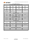
Table 6.1 USB2640/USB2641 Pin Descriptions (continued)
NAME SYMBOL
48-PIN
QFN
BUFFER
TYPE DESCRIPTION