


Ultra Fast USB 2.0 Multi-Format Flash Media Controller/USB Hub Combo
Revision 2.0 (10-03-08) 54 SMSC USB2640/USB2641
DATASHEET
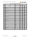
Chapter 9 DC Parameters
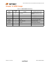
9.1 Maximum Guaranteed Ratings
Note 9.1 Stresses above the specified parameters may cause permanent damage to the device.
This is a stress rating only. Functional operation of the device at any condition above those
indicated in the operation sections of this specification is not implied.
Note 9.2 When powering this device from laboratory or system power supplies the Absolute
Maximum Ratings must not be exceeded or device failure can result. Some power supplies
exhibit voltage spikes on their outputs when the AC power is switched on or off. In addition,
voltage transients on the AC power line may appear on the DC output. When this
possibility exists, a clamp circuit should be used.
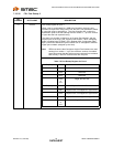
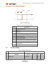
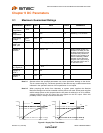
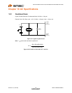
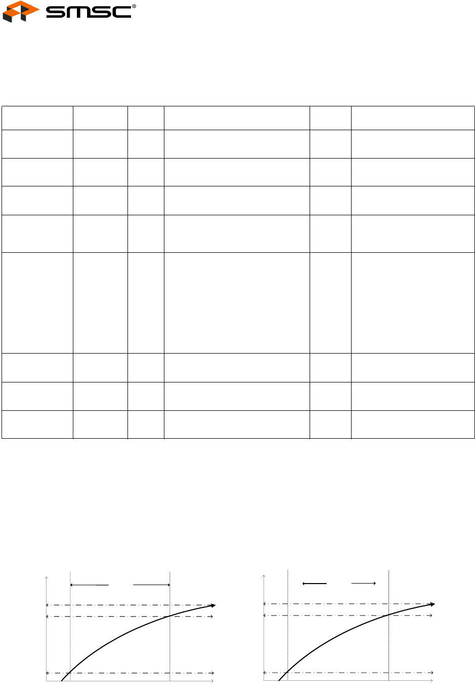
Figure 9.1 Supply Rise Time Models
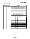
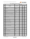
PARAMETER SYMBOL MIN MAX UNITS COMMENTS
Storage
Temperature
T
STOR
-55 150 °C
Lead
Temperature
325 °C Soldering < 10 seconds
3.3V supply
voltage
V
DD33,
V
DDA33
-0.5 4.0 V
Voltage on
USB+ and
USB- pins
-0.5 (3.3V supply voltage + 2) ≤ 6V
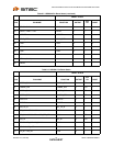
Voltage on
GPIO10
-0.5 V
DD33
+ 0.3 V When internal power FET
operation of these pins are
enabled, these pins may be
simultaneously shorted to
ground or any voltage up to
3.63V indefinitely, without
damage to the device as
long as V
DD33
and V
DDA33
are less than 3.63V and T
A
is less than 70
o
C.
Voltage on
any signal pin
-0.5 V
DD33
+ 0.3 V
Voltage on
XTAL1
-0.5 3.6 V
Voltage on
XTAL2
-0.5 2.0 V
t
10%
10%
90%
Voltage
t
RT
t
90%
Time
100%
3.3V
VSS
VDD33
t
10%
10%
90%
Voltage
t
RT
t
90%
Time
100%
1.8V
VSS
VDD18