


H
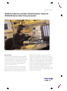
DMI Compliance & Sink Characterization Using DTG5000 Series Data Timing Generator
Application Note
4
www.tektronix.com/signal_sources
4
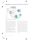
Most HDMI product developers want to perform
pre-compliance testing; they have a clear incentive to
ensure interoperability and compatibility. While it is
recommended to perform as many tests as possible,
certain core tests are an essential part of compliance.
T
able 2 summarizes some of the above core tests.
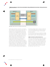
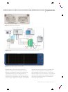
Transmitter or Source signal characteristics can be
effectively characterized by measuring signals at test
point TP1 to ensure that they are within standard
timing, jitter and voltage margins.
The oscilloscope is of course the key platform for
observing signals at these test points. The digital
storage oscilloscopes (DSO) and digital phosphor
oscilloscopes (DPO) in the Tektronix TDS family
can be pair
ed with the TDSHT3 application softwar
e
package for HDMI work. TDSHT3 provides accurate
automated Sour
ce measur
ements for HDMI compliance,
including those summarized in Table 2. For more
information about this subject, refer to the Tektronix
application note titled Physical Layer Compliance
Testing for HDMI Using TDSHT3 HDMI Compliance
Test Software (available at wwww.tektronix.com).
This balance of this technical brief will concentrate on
the equipment and procedures for compliance and
characterization measurements on HDMI Sink devices
and cables.
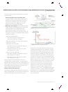
HDMI Sink T
ests
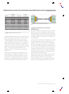
Jitter Tolerance
One of the most critical characteristics of a Sink
device is its tolerance to jitter in the incoming signal.
The HDMI standard defines the limit as 0.3 x T
BIT
; the
ter
m T
BIT
is HDMI syntax for “unit inter
val.” The test
approach is straightforward: specified amounts of jit-
ter are injected in steps into the transmitted TMDS
signal. Each step increases the jitter amount from low
to high until the sink device fails to r
ecover the signal.
The amount of jitter at which this failure occurs is
compar
ed against the published limits for compliance.
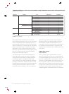
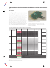
Electrical Signals Test CTS Test ID Test Point
Source Clock and/or Data Data Eye Diagram 7-10 TP1
Clock Jitter 7-9 TP1
Clock Duty Cycle 7-8 TP1
Overshoot/Undershoot 7-5 TP1
Rise/Fall Time 7-4 TP1
I
nter-pair Skew 7-6 TP1
Data-Data Inter-pair Skew 7-6 TP1
S
ingle-ended Intra-pair Skew 7-7 TP1
Low Level Output Voltage (VL) 7-2 TP1
S
ink Jitter Tolerance 8-7 TP2
Minimum Differential Sensitivity 8-5 TP2
Intra-pair Skew 8-6 TP2
Differential Impedance 8-8 TP2
Cable Data Eye Diagram 5-3 TP1, TP2
Table 2.
Core HDMI tests.