


Jumpers
3-3
Operation
3.1.1 JMP1: Short R1
In order to allow current output IDAC0 to have full compliance, JMP1 can
be used to short out resistor R1, which is in series with that signal.
3.1.2 JMP2: Short R2
In order to allow current output IDAC0 to have full compliance, JMP2 can
be used to short out resistor R2, which is in series with that signal.
3.1.3 JMP3: I
2
C Data SDA Enable
The MSC1211 uses the same signals for SPI and I
2
C. Since there is no chip
select available for the I
2
C device, this jumper will allow the isolation of the
256K EEPROM during SPI testing.
3.1.4 JMP3: I
2
C Data SCL Enable
The MSC1211 uses the same signals for SPI and I
2
C. Since there is no chip
select available for the I
2
C device, this jumper will allow the isolation of the
256K EEPROM during SPI testing.
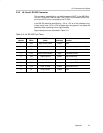
3.1.5 JMP5: AV
DD
Power Source Select
The MSC1211 has separate analog and digital power supplies. Use JMP5 to
connect the desired voltage source for the analog power supply AV
DD
. Short-
ing pins 1 and 2 connects the onboard 5V regulator. Pins 2–3 can be used to
supply an external voltage for use as AV
DD;
pin 2 is for the external voltage and
pin 3 is for AGND.
3.1.6 JMP6: DV
DD
Power Source Select
The MSC1211 has separate analog and digital power supplies. Use JMP6 to
connect the desired voltage source for the digital power supply DV
DD
. Shorting
pins 1 and 2 connects the onboard 5V regulator. Pins 2–3 can be used to sup-
ply an external voltage for use as DV
DD;
pin 2 is for the external voltage and
pin 3 is for AGND.
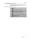
3.1.7 J7: Reference Select
J7 has six pins. For normal operation pins 1 and 2 are connected for REF IN–
to be connected to AGND. Since the MSC1210 has a very similar pinout to the
MSC1210, the MSC1211 board is designed to accommodate the MSC1210
device. For the MSC1210, the VDAC1 pin is the REFOUT pin. Therefore, a
connection between pins 3 and 4 will provide the other required connection for
use of the internal reference for the MSC1210. Only pins 1 and 2 are needed
for the MSC1211. Pins 4 and 6 can be connected together, if you want to use
AV
DD
as the reference voltage.
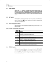
3.1.8 J16: Memory Configuration
The MSC1211EVM can use either RAM or EEPROM in the socket for U9. The
J16 jumper provides the capability to configure the Addressing and Write En-
able signals for each use. For use with compatible EEPROMs, the following pins
are shorted: 1–2, 3–5 and 4–6. For use with the RAM memory that comes stan-
dard on the MSC1211EVM, the following pins are shorted: 1–3, 2–4, 5–6.