


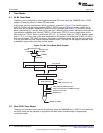

INVINP_LO
CLKSRC_LO
Internalclock
Gated
internalclock
TINPL
Externalclock
TIEN_LO
01
0
1
Inputclock
totimer
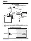
Timer Operation
www.ti.com
3.3 Timer Clock Source Selection
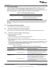
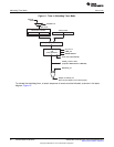
As shown in Table 4 and Figure 8, the timer clock source for TIMLO is selected using the clock source
(CLKSRC) bit and timer input enable (TIEN_LO) bit in timer control register (TCR). The input clock source
for TIMHI is always the internal clock(except C6472/TCI6486 devices). For C6472/TCI6486 devices, bit 24
and bit 25 are used to select the clock source to be internal or external for TIMHI.
Three clock sources are available to drive the timer clock:
• The internal clock, by setting CLKSRC_LO = 0 and TIEN_LO = 0.
• The internal clock gated by the timer input signal, by setting CLKSRC_LO = 0 and TIEN_LO = 1.
• The external clock on the timer input pin (TINPL), by setting CLKSRC_LO = 1. This input signal is
synchronized internally and can be inverted by setting the timer inverter control (INVINP_LO) bit in
TCR to 1.
At reset, the clock source is the internal clock. The internal clock is derived from the DSP clock generator,
as shown in Figure 2.
When the clock source is the gated internal clock, the timer starts counting when the timer input transitions
from low to high and the timer stops counting when the timer input transitions from high to low.
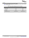
Table 4. Timer Clock Source Selection
CLKSRC_LO TIEN_LO Input Clock
0 0 Internal clock (default)
0 1 Gated internal clock
1 X External clock on timer input (TINPL)
Figure 8. Timer Clock Source Block Diagram
3.4 Timer Output Mode Selection
The two basic timer output modes are pulse mode and clock mode. The timer output mode is selected
using the clock/pulse mode bits (CP_LO and CP_HI) in the timer control register (TCR).
When in the pulse mode (CP_LO or CP_HI = 0), the pulse width bits (PWID_LO or PWID_HI) set the
pulse width to 1, 2, 3, or 4 timer clock cycles. This pulse can be inverted by setting the timer output
inverter control bits (INVOUTP_LO or INVOUTP_HI) to 1.
When in the clock mode (CP_LO or CP_HI = 1), the timer output signal has a 50% duty cycle. The signal
toggles (from high-to-low or from low-to-high) each time the timer counter reaches the timer period.
The output signal of TIMLO is driven on both TSTAT_LO and the timer output pin TOUTL. The output
signal of TIMHI is driven on TSTAT_HI only.
14
C6472/TCI648x 64-Bit Timer SPRU818B–December 2005–Revised September 2010
Submit Documentation Feedback
Copyright © 2005–2010, Texas Instruments Incorporated