TPS62065/67EVM-347 Assembly Drawings and Layout
www.ti.com
7 TPS62065/67EVM-347 Assembly Drawings and Layout
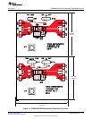
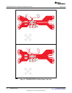
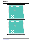
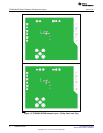
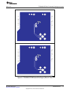
Figure 12 through Figure 16 show the design of the TPS62065/67EVM-347 printed circuit boards. This
EVM has been designed using a four-layer, 1-ounce copper-clad PCB (3.81 cm by 4.57 cm) with all
components in an active area on the top side of the board. All active traces to the top and bottom layers to
allow the user to easily view, probe, and evaluate the TPS62025/67 control ICs in a practical,
double-sided application environment. Moving components to both sides of the PCB or using additional
internal layers can offer additional size reduction for space-constrained systems.
NOTE: Board layouts are not to scale. These figures are intended to show how the board is laid
out; they are not intended to be used for manufacturing TPS62065/67EVM-347 PCBs.
12
TPS62065/67EVM SLVU364–March 2010
Submit Documentation Feedback
Copyright © 2010, Texas Instruments Incorporated


