


38
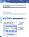
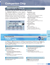
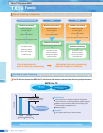
The TMPR4937XBG is based on a TX49/H3 core, and contains a
PCI controller, a DMA controller, a memory controller, a UART, a
timer and other peripherals. It is a 64-bit RSC microcomputer well
adapted to networks and digital information appliances. The
processor operates at frequencies of 300 MHz and 333 MHz, while
the PCI bus runs at a frequency of 33/66 MHz.
● TX49/H3 64-bit RISC core
● On-chip caching
Four-way set-associative caches
Instruction cache: 32 Kbytes
Data cache: 32 Kbytes
Cache lock function
● Memory management unit (TLB): 64 entries
4 K / 16 K / 64 K / 256 K / 1 M / 4 Mbyte pages
● Memory controller: SDRAM (64-bit, 133 MHz)
SRAM, ROM, NOR Flash and I/O
● Interrupt controller: 6 external sources
● 32-bit timer: 3 channels
● UART: 2 channels
● PCI controller (32-bit, 33/66 MHz)
● DMA controller: 8 channels
● AC-Link (AC97 interface)
● I/O ports: 16-bit
● Maximum operating frequency: 300/333 MHz
● I/O supply voltage: 3.3 V
Internal supply voltage: 1.5 V
● Package: 484-pin PBGA
(with 64-pin thermal balls)
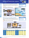
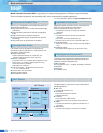
TX49/H3 core
Debug Support Unit (DSU)
Data Cache
(32K)
Instruction
Cache (32K)
IU
MMU
BIU
Write
Buffer
Floating-Point Unit (FPU)
G BUS Interface
General
Purpose
Register
MAC unit
64-bit
G-BUS
Clock Generator
SDRAM Controller
External Bus Interface
DMA Controller
PCI Controller
IM BUS Bridge
AC-Link
UART Timer Parallel I/O
Interrupt
Controller
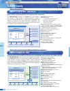
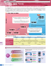
TMPR4937XBG-300/333
Built-in PCI controllers
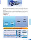
TMPR4926XB-200
Built-in PCI controller, Encoder (DES) and NAND Flash controller
64-bit RISC microprocessor with built-in PCI controller
General-purpose 64-bit RISC microprocessor with NAND Flash controller, PCI, DMA and DES
TX49 Family
64-Bit TX System RISC
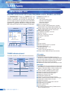
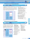
The TMPR4926XB-200 is a 64-bit RISC microcomputer that is based
on a TX49/H2 processor core and contains a NAND flash controller,
a PCI controller, a memory controller, a UART, a timer, a DES and
other peripherals. It supports a TX49/H2 core suitable for high-speed
mode. The processor operates at a frequency of 200 MHz, while the
PCI bus runs at a frequency of 33 MHz.
● Instruction cache: 16 Kbytes
(4-way set-associative caches)
● Data cache: 16 Kbytes
(4-way set-associative caches)
● MAC: Multiply-accumulate
● Memory management unit (TLB):
48 double entries (odd/even)
Joint TLB, 4 K/16 K/64 K/256 K/1 M/4 M bytes pages
● Memory controller:
Supports NAND Flash, SDRAM (32-bit, 80 MHz),
SRAM, ROM, NOR Flash and I/O
● Interrupt controller: 8 external sources
● 32-bit timer: 3 channels
● UART: 2 channels
● SPI
● PCI controller (32-bit, 33 MHz)
● DMA controller: 4 channels
● PCMCIA: 2 slots
● AC-Link (AC97 interface)
● Real-time clock
● CHI
●
DES/3DES (Data Encryption Standard: Encoder)
● I/O port: 32-bit
● RF (Reduced Frequency) function
● Maximum operating frequency: 200 MHz
● I/O supply voltage: 3.3 V
Internal supply voltage: 1.5 V
● Package: 256-pin PBGA (27 x 27 mm)
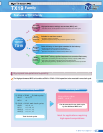
TX49/H2 core
Debug Support Unit (DSU)
Data Cache
(16K)
Instruction
Cache (16K)
IU
MMU
BIU
Write
Buffer
Floating-Point Unit (FPU)
G BUS Interface
General
Purpose
Register
MAC unit
32-bit
G-BUS
AC-Link
UART Timer SPI RTC
Parallel
I/O
Interrupt
Controller
NAND FLASH Controller
SDRAM Controller
External Bus Interface
DMA Controller
PCI Controller
PCMCIA Interface
CHI
Data Encryption Standard
(
DES
)
IM BUS Bridge