


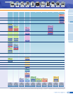
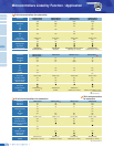
31
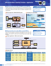
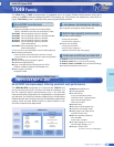
Applications
LCD display
TMP86C420
TMP86C820
TMP86C822
TMP86C829B
TMP86CH21A
TMP86CH22
TMP86CH29B
TMP86CM23A
TMP86CM29
TMP86CM25
AF control (computation),
AE control (computation)
Built-in strobe control
Dial input, shutter control
TMP1942CYU
TMP1942CZU
TMP1942CZXB
Camera control/Shutter control
AF control/Tape control
TMP1962C10BXB
TMP19A64F20BXB
TMP19A64C1DXB
TMP19A43FDXB
TMP19A43FZXB
TMP19A43CDXB
TMP19A43CZXB
TMP86FM26
TMP86CP23A
TMP86FP24
TMP86CS25A
TMP86CS28
TMP86FS28
These microcontrollers incorporate high-speed AD converters to support
AF/AE control (computation), dial input, and other features suitable for the
main controller of a single-lens reflex camera.
■
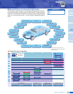
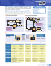
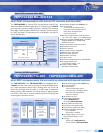
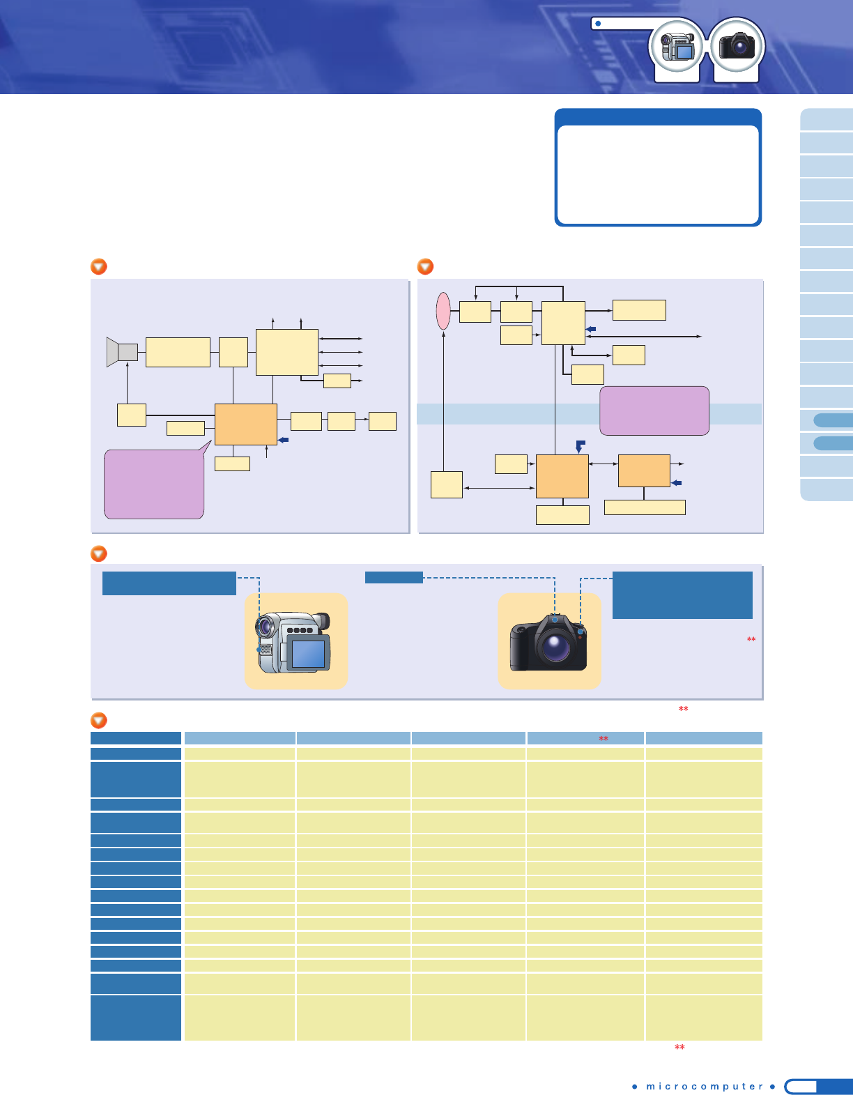
Microcontrollers for digital single-lens reflex cameras (DSLRs)
These microcontrollers, responsible for controlling the camera and tape deck
sections, contain large-capacity ROM to help minimizing the product size and
support various features suitable for main DVC control.
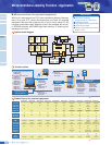
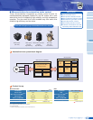
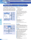
■ Microcontrollers for digital video cameras (DVCs)
LENS
Zoom
Motor
EEPROM
Large-scale software
that controls the camera
and deck blocks.
Multipin system control
interface
High performance,
low power dissipation
A single chip controls
both the camera and
deck blocks.
Analog Font End
Camera
DSP
Memory Card
USB
IEEE1394
In-out
LCD panelLCDC
OPAMP
Motor
Drive
DECK
System
microcontroller
TMP1962
TMP19A64
Flash Key
Audio
DV control
LSI
Video
Image processing system
Timing signal
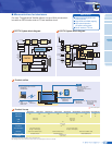
AF control
Shutter control
Iris control
Signals
Camera control system
Analog
front
end
USB
IEEE1394
Wireless,
infrared ray
Battery control
AE
Sensor
AF
Sensor
DRAM
Camera
Key/switch
Information display LCD
LCD
microcontroller
Memory
card
Lens
micro-
controller
Image display
LCD
System
microcontroller
DSC signal
processing
LSI
(CUSTOM)
SoC
For image processing engine
For display system
For main processing in camera control system
TLCS-870/C
Area
Sensor
TMP1942
TMP19A43
Independent image processing
and camera control systems
run in parallel.
Faster image processing
High-speed multipoint AF
DVCs DSLRs
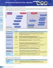
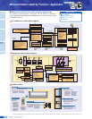
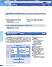
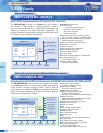
Part Number
Maximum operating frequency (MHz)
32
TMP1942CYUG/CZUG/CZXBG
Internal bus width 32
External bus width
16 (address/data
multiplexed)
Internal ROM (bytes) 256/384K
Internal RAM (bytes) 16K
DMAC channels 4ch
I/O ports 108
Serial interface 6ch
Timer channels 28ch
External interrupt pins
29
Dual clock ●
Debug support unit ● (Flash product only)
Package
LQFP144(16 x 16mm)/
FBGA177(13 x 13mm)
40.5
Supply voltage (V)
2.7 to 3.6
1.35 to 1.65
I/O: 1.65 to 3.3
2.3 to 3.3
AD: 2.7 to 3.5
TMP1962C10BXBG
32
16
(multiplexed or
separate selectable)
1024K
AD converter 16ch (conversion time: 2µs) 24ch
40K
8ch
202
8ch
18ch
25
●
FBGA281(13 x 13mm)
Others
10-bit DA converter x 3 channels
ROM correction
2-phase pulse input counter
Dynamic pull-up
5 V capable ports (x 15)
ROM correction
2-phase pulse input counter
-
40
1.35 to 1.65
I/O, AD
: 2.7 to 3.6
DA
: 2.3 to 2.7
TMP19A43FDXBG/CDXBG
32
16
(multiplexed or
separate selectable)
512K
16ch (conversion time: 1.15µs)
24K
8ch
143
7ch
17ch
48
●
FBGA193(12 x 12mm)
8-bit DA converter x 2 channels
ROM correction
2-phase pulse input counter
Dynamic pull-up
●
40
1.35 to 1.65
I/O, AD
: 2.7 to 3.6
DA
: 2.3 to 2.7
TMP19A43FZXBG /CZXBG
32
16
(multiplexed or
separate selectable)
384K
16ch (conversion time: 1.15µs)
20K
8ch
143
7ch
17ch
48
●
FBGA193(12 x 12mm)
8-bit DA converter x 2 channels
ROM correction
2-phase pulse input counter
Dynamic pull-up
●
54
1.35 to 1.65
I/O: 1.65 to 3.3
TMP19A64F20BXBG/C1DXBG
32
16 (multiplexed or
separate selectable)
2048K/1536K
24ch
64K/56K
8ch
209
8ch
12ch
20
●
FBGA281(13 x 13mm)
Built-in back-up block
ROM correction
2-phase pulse input counter
●
*
For details of the products listed above, see the "Part Number List".
: Under development
: Under development
● AF/AE control
(high-speed AD/multidigit operation)
● Dial input control
● Shutter control
● Tape control
● LCD display control
Main functions
Product line-up
Product outline
DVC system block diagram
DSLR system block diagram