


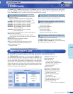

35
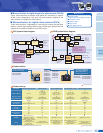
The TX49 Family of RISC microprocessors for embedded use is an original Toshiba 64-bit processor family and is
based on the RISC architecture designed by MIPS Technologies, Inc. The customer can implement a custom SoC us-
ing the TX49 Family cores in conjunction with general-purpose ASSP products.
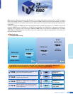
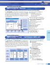
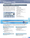
TMPR4951BFG-200
First product incorporating the TX49/L3 core
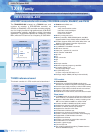
TX49 Family
64-Bit TX System RISC
64-bit RISC architecture Low-power consumption design
Built-in high-capacity primary cache
Can be used as a CPU core for custom SoC
● Instruction cache: 32 Kbytes
■
4-way set-associative
■
Lock function supported
● Data cache: 32 Kbytes
■
4-way set-associative
■
Lock function supported
■
Write-back/write-through (every page)
●
Low-power consumption modes (Doze/Halt)
● TX49/H2: 0.18-µm process technology
● TX49/H3, TX49/L3: 0.13-µm process technology
● TX49/H4, TX49/L4, TX49/W4: 90-nm process technology
● Complete development environment
● R4000A architecture
■
Upward-compatible instruction set including MIPS I,
MIPS II and MIPS
III
instruction set architectures (ISAs)
● TX49/H2: Internal operating frequency: 200 MHz
● TX49/H3: Internal operating frequency: 300 MHz/333 MHz
● TX49/H4: Internal operating frequency: 400 MHz
● TX49/L3: Internal operating frequency: 200 MHz
● TX49/L4: Internal operating frequency: 333 MHz
(Under development)
● TX49/W4: Internal operating frequency: 400 MHz
(Under development)
■
Level 2 cache of up to 256 Kbytes can be installed (optional)
● Non-blocking load function
■
The instructions which follow the instruction currently
be
ing executed are executed while the cache is being refilled.
● DSP function
● Thirty-two 64-bit general-purpose registers
● Optimized 5-stage pipelining
● Single- or double-precision floating-point unit (FPU)
(TX49/H2, TX49/H3, TX49/H4 and TX49/W4 core)
● Debug support unit (DSU)
■
Supports EJTAG.
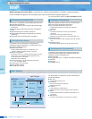
64-bit RISC microprocessor offering excellent cost performance
The TMPR4951BFG incorporates a 0.13-µm process TX49/L3 core,
and by minimizing the built-in functions and external interfaces, it of-
fers the industry's highest cost-performance ratio in the 200 MHz
class and low-power consumption, all encapsulated in a compact pack-
age. Moreover, the SysAD bus interface adopted for this microprocessor
enables diverted use of existing resources and facilitates system devel-
opment. These and other features make it an ideal controller for low-
end LBPs, networks, and settop boxes.
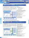
● TX49/L3 64-bit RISC core
● Five-stage pipeline
● On-chip caching
4-way set-associative caches
Instruction cache: 16 Kbytes built in
Data cache: 8 Kbytes built in
Cache lock function
● 48 double-entry
● External bus (32-bit SysAD bus)
● Low-power consumption mode
● Debug support unit (DSU) built in
(execution control only)
● Maximum operating frequency:
Core: 200 MHz
External bus: 100 MHz
● I/O supply voltage: 2.5 V or 3.3 V
Internal supply voltage: 1.5 V
● Package: 100-pin LQFP
(14 mm x 14 mm, 0.5-mm pitch)
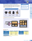
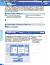
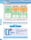
TX49/L3 Core
Integer Arithmetic
Unit
System Control
Coprocessor
Clock
Generator
64-Bit
General-
Purpose
Registers
Pipeline
Control
Integer
Arithmetic
Data Path
Multiplier/
Accumulator
Unit
Coprocessor
Registers
Memory Management
Unit
48 Double-Entry TLBs
Exception
Handling Unit
16-KB 4-Way
Set-Associative
Instruction Cache
8-KB 4-Way
Set-Associative
Data Cache
Cache
Controller
Write
Buffer
Sync Circuit
Debug
Support Unit
(EJTAG)
SysAD Bus
Interface