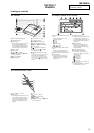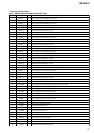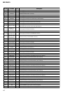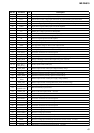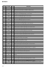
MZ-RH910
2424
MZ-RH910
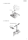
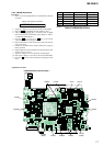
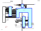
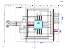
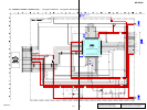
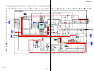
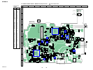
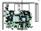
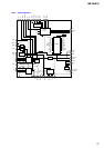
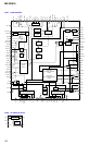
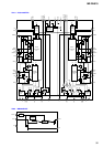
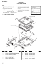
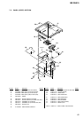
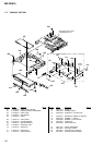
• Note For Printed Wiring Boards and Schematic Diagrams
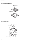
• MAIN board is multi-layer printed board.
However, the patterns of intermediate-layer have not been in-
cluded in this diagrams.
• Lead Layouts
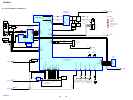
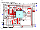
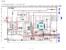
Note on Schematic Diagram:
• All capacitors are in µF unless otherwise noted. (p: pF)
50 WV or less are not indicated except for electrolytics
and tantalums.
• All resistors are in Ω and
1
/
4
W or less unless otherwise
specified.
• f : internal component.
• C : panel designation.
• A : B+ Line.
• Power voltage is dc 1.5 V and fed with regulated dc power
supply from battery terminal.
• Voltages and waveforms are dc with respect to ground
under no-signal conditions.
no mark : PLAYBACK
∗ : Impossible to measure
• Voltages are taken with a VOM (Input impedance 10 MΩ).
Voltage variations may be noted due to normal produc-
tion tolerances.
• Waveforms are taken with a oscilloscope.
Voltage variations may be noted due to normal produc-
tion tolerances.
• Circled numbers refer to waveforms.
• Signal path.
E : PLAYBACK
j : REC
J : OPTICAL IN
F : LINE IN
d : USB input from PC
G : USB output to PC
N : MIC IN
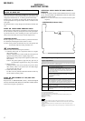
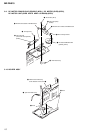
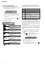
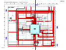
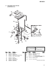
Note on Printed Wiring Board:
• X : parts extracted from the component side.
• Y : parts extracted from the conductor side.
• f : internal component.
• : Pattern from the side which enables seeing.
(The other layers' patterns are not indicated.)
Caution:
Pattern face side: Parts on the pattern face side seen from
(Conductor Side) the pattern face are indicated.
Parts face side: Parts on the parts face side seen from
(Component Side) the parts face are indicated.
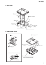
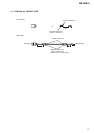
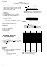
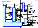
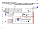
Lead layout of conventional IC
CSP (chip size package)
• The voltage and waveform of CSP (chip size package)
cannot be measured, because its lead layout is different
form that of conventional IC.
*Replacement of IC401, IC501, IC601 and IC801 used in
this set requires a special tool.
*Replacement of IC401, IC501, IC601 and IC801 used in
this set requires a special tool.
surfac
Note:
The components identi-
fied by mark 0 or dotted
line with mark 0 are criti-
cal for safety.
Replace only with part
number specified.
Note:
Les composants identifiés par
une marque 0 sont critiques
pour la sécurité.
Ne les remplacer que par une
pièce portant le numéro
spécifié.
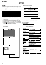
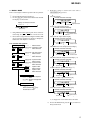
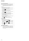
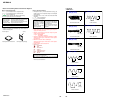
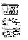
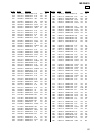
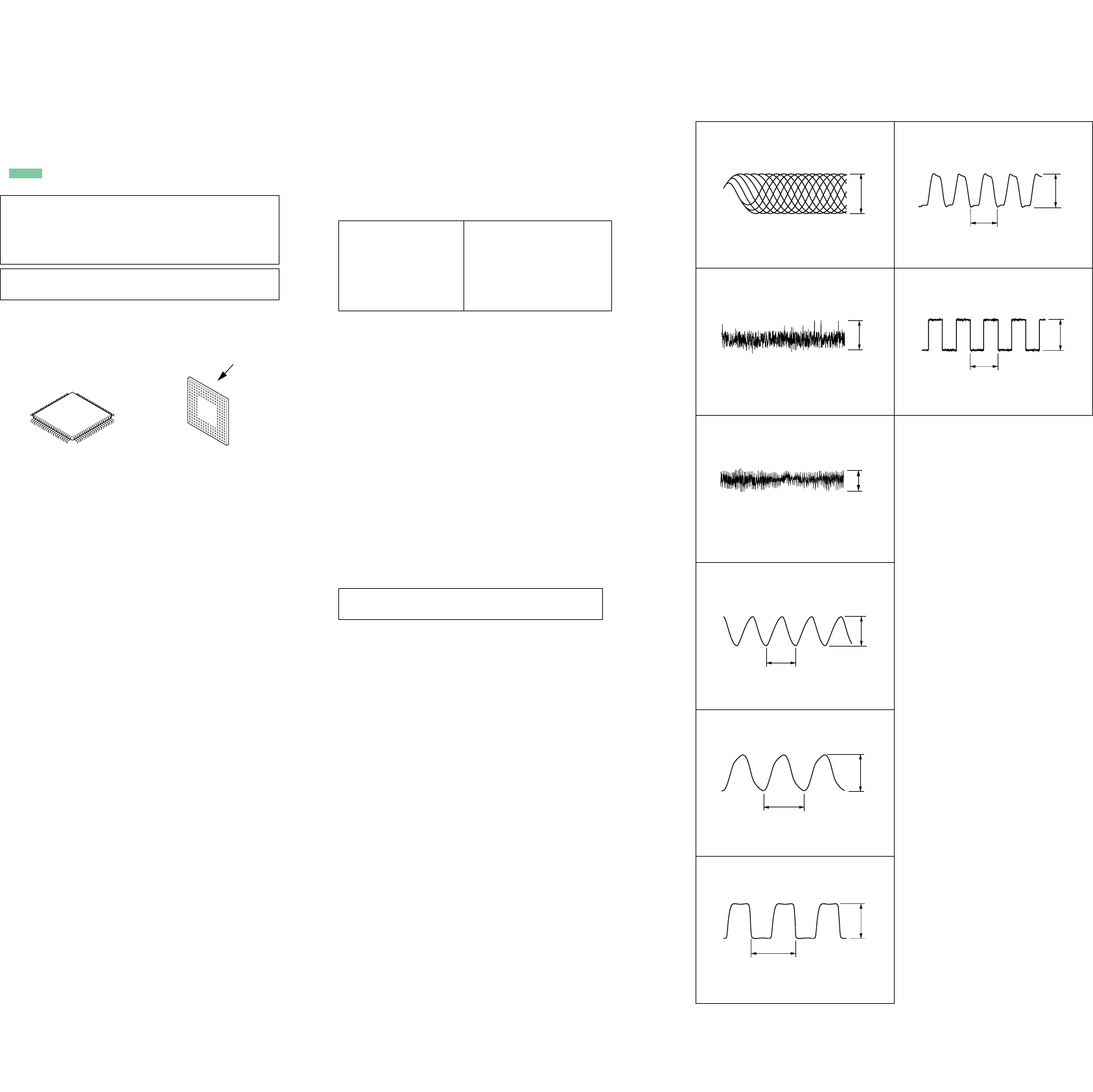
• Waveforms
– MAIN Board –
2
IC501 ra (FE)
(MD play mode)
100 mV/DIV, 500 ns/DIV
Approx.
280 mVp-p
1
IC501 8 (RFO)
(MD play mode)
500 mV/DIV, 500 ns/DIV
1.0 Vp-p
3
IC501 rs (TE)
(MD play mode)
200 mV/DIV, 500 ns/DIV
Approx.
100 mVp-p
4
IC351 6 (MCK)
1 V/DIV, 20 ns/DIV
44.3 ns
1.8 Vp-p
6
IC801 <czz (OSCO)
1 V/DIV, 20 ns/DIV
44.3 ns
2.6 Vp-p
7
IC301 8 (BCLK)
1 V/DIV, 100 ns/DIV
354 ns
2.2 Vp-p
88 ns
2.5 Vp-p
8
IC301 9 (MCLK)
1 V/DIV, 50 ns/DIV
22.8
µ
s
2,3 Vp-p
9
IC301 q; (LRCK)
1 V/DIV, 10
µ
s/DIV