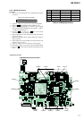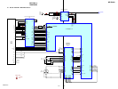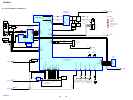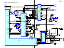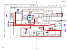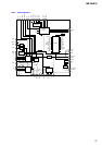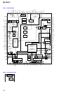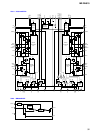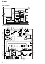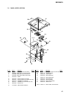
46
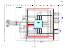
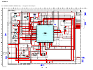
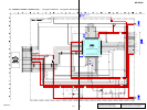
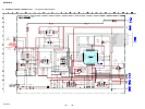
MZ-RH910
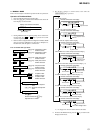
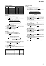
Pin No.
Pin Name I/O Description
247
CS_RTC O Chip select signal output to the real time clock Not used
248
JOG_A I Jog dial pulse input terminal (A phase)
249
JOG_B I Jog dial pulse input terminal (B phase)
250
VBUS_DET I Detection terminal of USB power supply
251
SSB_DATA I/O SSB data input/output with the RF amplifier
252
SSB_CLK O SSB clock output to the RF amplifier
253
UMD_PROTECT
I Recording protector for Hi-MD disc detection switch input terminal
254
LDPEN O Pulse/DC light-emit selection signal output to the optical pick-up block
255
CHG_TYPE2 O Charge control signal output terminal "H": charging
256
DRAM_HOLD
_DET
I Detection terminal for internal D-RAM power supply information keeping
257
DRAM_VDD_CLR
O Internal D-RAM power supply latch clear signal output for quick mode sleep
258
AD2ENDF I Monitor input terminal for flag of servo signal A/D measuring finish
259
TEST I Input terminal for the test Not used
260
SRAM_MODE I Terminal for setting
261
HSALF I Terminal for setting
262 to 271
MON0 to MON9 O Trigger monitor terminal Output clock=18.5 MHz
272
XLSRCK O Pulse output for laser strobe recording to the optical pick-up
273
TAT I Not used
274
TAN I Not used
275
NAR I Not used
276
IDO I Not used
277
SAK O Not used
278
LRCKI I L/R sampling clock signal input terminal for PCM data interface Not used
279
XBCKI I Bit clock signal input terminal for the PCM data interface Not used
280
DATAI I Serial data input terminal for the PCM data interface Not used
281
SI3 I Serial data input for LAM microcomputer communication Not used
282
SO3 O Serial data output for LAM microcomputer communication Not used
283
SCK3 O Serial data transfer clock signal output for LAM microcomputer communication Not used
284
SI4 I Serial data input for ATRAC3 plus encoder communication Not used
285
SO4 O Serial data output for ATRAC3 plus encoder communication Not used
286
SCK4 O Serial data transfer clock signal output for ATRAC3 plus encoder communication Not used
✶✼✼
287,
NC - Not used
289
HI_Z_SLD O Standby signal output for the sled motor to the motor driver
290
HI_Z_SPDL O Standby signal output for the spindle motor to the motor driver
291 to 294
SET_CODE0 to
SET_CODE3
I Input terminal for the model setting
295, 296
D_EN1, D_EN2 O Headphone/LINE/beep selection signal output to the headphone amplifier Not used
297
D_ENVG O Power on/off control signal output terminal for headphone amplifier
298
DADT O Audio data output to the D/A converter Not used
299, 300
PWM_L1,
PWM_L2
O LC drive PWM output terminal Not used
301, 302
I2C_1, I2C_2 I/O Open drain for I2C
303, 304
JTAG0, JTAG1 I/O Terminal for setting
305
CLKIN2 I Clock signal input terminal (13.5 MHz or 27 MHz) Not used
306
FS256 O Master clock signal (256Fs=11.2896 MHz) output to A/D converter
307
ADDT I Data input from A/D converter
308
LRCK O L/R sampling clock signal (44.1kHz) output to external A/D converter