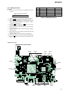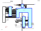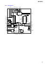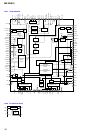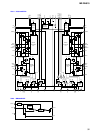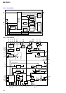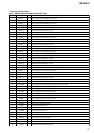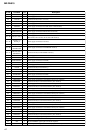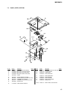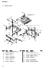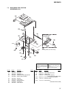
45
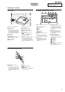
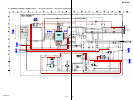
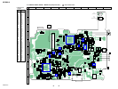
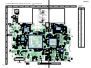
MZ-RH910
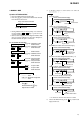
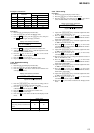
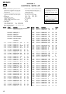
Pin No.
Pin Name I/O Description
199
BEEP O Beep sound control signal output to the headphone amplifier Not used
200
XOPT_CTL O Power supply on/off control signal output terminal for the optical input jack
201
NC - Not used
202
EL_PWR_CTL O EL power supply on/off control signal output terminal Not used
203
REC_LED/
ACCESS_LED
O Recording indication LED and accessing indication LED drive signal output terminal Not used
204
MDVCC_CTL O Power supply control signal output terminal for the optical pick-up block
205
VBUS_VB_CTL O USB power supply control signal output terminal
206
EL_PWR_CTL O EL VDD power supply on/off control signal output terminal Not used
207
DRAM_ALONE O Power on/off control signal output terminal for internal D-RAM
208
XNV_WP_CTL - Write protect signal output to the EEPROM
209, 210
PD_S0, PD_S1 O PD IC mode selection signal output to the optical pick-up block
211
D_ENREG O Internal power supply on/off control signal output to the headphone amplifier
212
XMUTE O Muting on/off control signal output terminal
213
SI1 I Serial data input from the switch unit
214
SO1 O Serial data output to the switch unit
215
SCK1 O Serial data transfer clock signal output to the switch unit
216
SLD_MON I Monitor signal input terminal of sled servo
217
AOUT_SEL O Headphone/line output selection signal output terminal Not used
218
SLEEP O Chip enable signal output to the power control IC
219
FFCLR O Power supply on/off control signal output terminal for FCRAM (internal RAM)
220
NC - Not used
221, 222
CHGI_CTL2,
CHGI_CTL3
O Charge current control signal output terminal "H": low current charge
223
NC - Not used
224
XTEST I Input terminal for the test mode setting "L": test mode
225
XRF_RST O Reset signal output to the RF amplifier
226
VREC_SEL O VREC wake up timing control signal output terminal Not used
227
XHOLD_SW I HOLD switch input terminal
228
T_MARK_SW I T MARK switch input terminal Not used
229
XRST2_DET I Reset signal input from the power control IC
230
CHGI_SEL O Charge/discharge control signal output for current detection amplifier to the charge control IC
231
RECP_MON I Monitor input terminal for laser power selection signal output
232
SPDL_MON I Monitor signal input terminal of spindle servo
233
XCS_PWR_IC O Chip select signal output to the power control IC
234
USB_CHARGE O USB charge control signal output terminal
235
AC_CHARGE O AC charge control signal output terminal Not used
236
XCS_LCD O Chip select signal output to the switch unit
237
CC_CTL/VI_CTL
O Constant current circuit control signal output to the charge control IC
238
XRST_MTR_DRV
O Reset signal output to the motor driver
239
XCS_NV O Chip select signal output to the EEPROM
240
CHG_PWM O Charge current or voltage control signal output to the charge control IC
241
IAMP_CAL O Offset signal output for current detection amplifier charge control IC Not used
242
NC - Not used
243
D_VCONT_PWM
O For voltage control signal output to the headphone amplifier
244
CHG_OPR_LED
O Charging indication LED drive signal output terminal
245
XCS_REC_DRV
O Chip select signal output to the over write head driver
246
GND_SW O Ground line selection signal output terminal