


2 61433105L2-5DSection 61433105L2, Issue 4
capability that maintains data integrity across the carrier
facility. For subrate and 19.2 kbps rates, error correction
and data transmission is accomplished over a single DS0
time slot using a Majority Vote Error Correction
(MVEC) algorithm. For error correction at these rates,
MVEC must be selected in the BCU via the SLC Series 5
CIU.
For rates of 56 and 64 kbps, error correction requires one
additional DS0 time slot for the error correcting parity
byte. The Series 5 Total Reach DDS-DP only allows
SCEC, the parity byte error correction scheme, at 56 and
64 kbps. When error correction is desired for 19.2 kbps
service, provision 9.6 kbps and MVEC via the CIU and
select 19.2 on SW2.
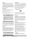
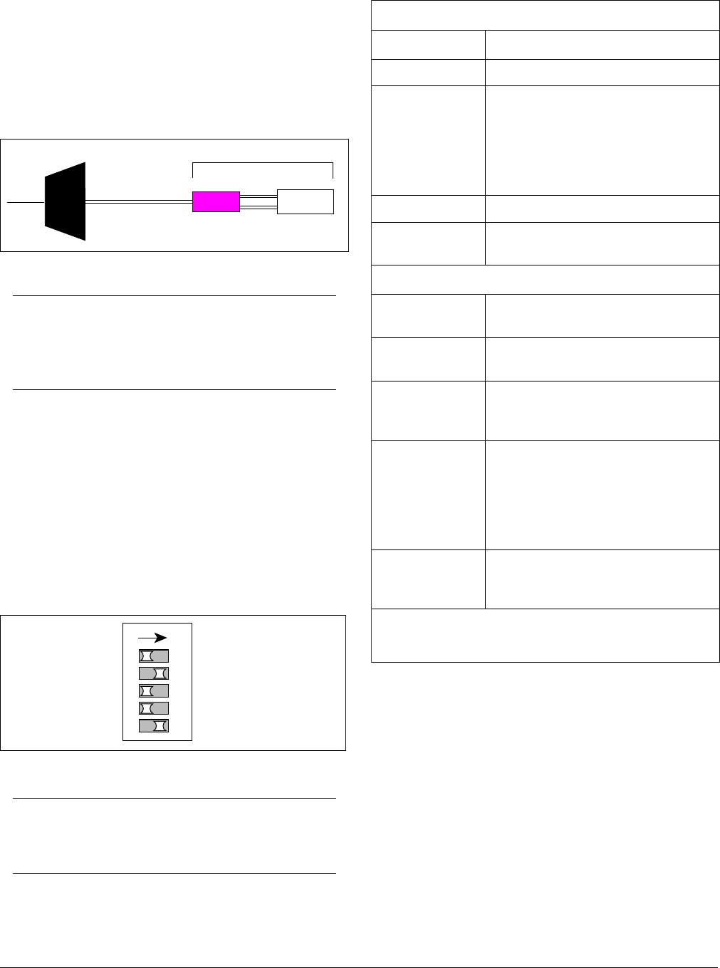
Series 5 Total Reach DDS-DP may interoperate over
the carrier system with another Total Reach DDS-DP,
OCU DP, DS0 DP, 1/0 DCS, or switch and may be
located in an end office, hub office, intermediate
office, or Digital Loop Carrier (Figure 2). The
2-wire loop is connected using the odd pair Tip (pin
31) and Ring (pin 32) on the Series 5 backplane.
NOTE
The Series 5 Total Reach DDS-DP must be
used with an appropriate Total Reach DDS-
R unit.
Options
The Series 5 Total Reach DDS-DP is provisioned
through the SLC Series 5 system and an on-board DIP
switch. SW2 provides feature options not available
through the SLC Series 5 channel bank intelligent
system. Use the SLC Series 5 Craft Interface Unit (CIU)
to provision intelligent channel bank features supported
by the Series 5 Total Reach DDS-DP. See Figure 3
and Table 1 for option description and provisioning.
NOTE
Select OCU DP, CLEI 5SCU48, when
provisioning via the CIU.
Error Correction
When error correction is enabled the Series 5 Total Reach
DDS-DP provides an error detection and correction
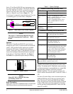
Table 1. Option Settings
UCB5seireSaivgninoisivorPerawtfoS
noitcnuFnoitpircseD
etaRspbk65ro,6.9,8.4,4.2tceleS
noitcerroCrorrE
)CE(
:tceles,2.91hguorht4.2sietarfI
elbaliavatonCECS(ENONroCEVM
).dracsihtnosetaresehtta
:tceles,spbk46hguorht65sietarfI
taA/NsiCEVM(ENONroCECS
).setareseht
)CZ(edoCoreZoNroseY
yradnoceS
)CS(lennahC
oNroseY
2WShctiwSpiDaivgninoisivorPerawdraH
K46)K46(1-2WS
lennahCraelCspbk46stcelesNO
K2.91
1
)K2.91(2-2WS
etarpool2.91stcelesNO
65dehctiwS)65WS(3-2WS
65dehctiwSselbaneNO
65dehctiwSselbasidFFO
gnilangiSB/A)GISBA(4-2WS
ehtfoetatsehtsenimretedtinuehtNO
slangisgnisustibgnilangisBdnaA
.enalpkcabknablennahcehtnotneserp
morfgnilangisseviredtinuehtFFO
.maertsatadgnimmocnieht
rotinoMytilauQ)MQ(5-2WS
MQselbaneNO
MQselbasidFFO
1
dna2WSno2.91tcelesnoitcerroCrorrEspbk2.91roF
.UIC5seireSCLShtiwCEVM6.9elbane
Figure 2. Total Reach DDS Circuit Diagram
T-Carrier
SLC
SERIES 5
DLC
2-Wire Loop
4-Wire Customer
Interface
DSU/CSU
TR
DDS-R
DDS-DP
T/R Pair
Customer Premises
TR
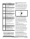
Figure 3. Option Switch
SW2
64K
19.2K
SW56
ABSIG
QM
1
ON
2345