54
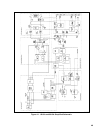
If the first pathway is taken, it is seen that primary power from the ac mains enters the INPUT RECTIFIER via the inrush
current limiting resistor. The rectifier converts the ac voltage to dc voltage and passes its output to the input filter. The unit
has a feature which allows it to operate either at 110/120 or 220/240Vac mains voltage. The voltage doubling capability as
it is called is effected by connecting jumper AlW1 between the rectifier and filter. When the mains voltage is 220/240Vac,
the jumper is open permitting the filter to develop a typical bus voltage of about 300Vdc. However, when the mains voltage
is 110/1120Vac, the jumper terminals are connected and the rectifier/filter combination now behaves as a voltage doubler
enabling a bus voltage of 300Vdc to be developed .
For the second pathway, primary power passes the Mains Voltage Select Switches to the BIAS POWER SUPPLIES which
provide the operating voltages for the internal circuits. The Mains Voltage Select Switches connect the primary windings of
the Bias-Supplies' transformer for operation at 120, 220, or 240Vdc.
The unit checks that the + 5Vdc bias voltage and the ac mains voltage are within acceptable limits as part of its turn-on
sequence.
DC Power Conversion Subsystem
The current available at the input rails after rectification enters the power transformer A1T2 and Primary Current Monitor
Transformer A1T1. This current flow is controlled by the FETs which act as high frequency switches. The FETs driver
circuits are under the control of the Pulse Width Modulator where the On/Off pulses originate.
During the on-pulse the FETs are turned on and current enters the primaries of transformers A1T1 and A1T2 as described
above. The output rectifiers A5CR4 and A5CR5 (6011A and 6015A) being reversed biased block the flow of current from
the secondary of A1T2 to the output. There is therefore a current build up and the secondary windings of A1T2 act as a
storage device. Meanwhile the current in the secondary of current transformer A1T1 develops a linearly increasing voltage
waveform across resistors A2R116 and A2R117. This waveform is the Ip Ramp Voltage and corresponds to the energy
build up in the secondary of the power transformer.
When the FETs are turned off, the collapsing magnetic field reverses the polarity across the power transformer causing the
output rectifiers to be forward biased. Current therefore flows from the secondary windings to the output filters.
Output Subsystem
As discussed above, power reaches the output rail when the FETs are turned off and the output diodes are forward biased.
The signal is first passed through the first stage of the output filter network where most of its 20KHz ripple derived from
the switching FETs are attenuated. Part of the signal leaving the first stage filter is fed back to the CV and CC Circuits as
the Innerloop Voltage Sense and becomes part of the inner control loop. The primary purpose of these feed-back loops is to
impart sufficient stability to the power supply and enable it to cope with a variety of loads.
The signal from the first stage filter also becomes the input to the second stage capacitor filter which provides the additional
filtering necessary for the unit to meet its specifications. This filter is close to + S and - S output terminals thereby ensuring
that the filter is as close to the user's load as possible. The output from the + S and - S terminals is also fed back to the CV
and CC Circuits and forms part of the outer feedback loop.
The 6015A units contain an A9 output board that provides protection against excessive reverse voltage applied across the
output terminals.
The Front Panel Board
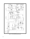
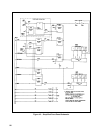
Figure 4-3 is a simplified schematic of the front panel board. The V-MON, I-MON, and OVP signals are passed to the front


