


ADP1148, ADP1148-3.3, ADP1148-5
–10–
REV. A
Design Example
As a design example, assume V
IN
= 12 V (nominal), V
OUT
= 5 V,
I
MAX
= 2 A, and f = 200 kHz, R
SENSE
. C
T
, and L can immedi-
ately be calculated:
R
SENSE
= 100 mV/2 = 50 m
Ω
t
OFF
= (1/200 kHz) × [1 – (5/12)] = 2.92
µ
s
C
T
= 2.92
µ
s/(1.3 × 10
4
) = 220 pF
L min = 5.1 × 10
5
× 50 E-3 Ω × 220 pF × 5 V = 28
µ
H
Assume that the MOSFET dissipations are to be limited to
P
N
= 2P
P
= 250 mW.
If T
A
= 50°C and the thermal resistance of each MOSFET is
50°C/W, then the junction temperatures will be 63°C and d
P
=
d
P
= 0.007 × (63–25) = 0.27.
The required R
DS(ON)
for each MOSFET can now be calculated:
P-Ch R
DS(ON)
= 12 × 0.25/5 × 2 × 1.27 = 120 m
Ω
N-Ch R
DS(ON)
= 12 × 0.25/7 × 2 × 1.27 = 85 m
Ω
The P-channel requirement can be met by a IRF7204. The
N-channel requirement can be met by a IRF7404. Note that
the most stringent requirement for the N-channel MOSFET is
with V
OUT
= 0 (i.e., short circuit). During a continuous short
circuit, the worst case N-channel MOSFET dissipation rises to:
P
N
~ I
SC(AVG)
2
× R
DS(ON)
× (1 + d
N
)
With the 50 mΩ sense resistor I
SC(AVG)
= 2 A will result, increas-
ing the N-channel dissipation to 0.45 W at die temperature of
73°C.
C
IN
will require an rms current rating of at least 1 A at tempera-
ture, and C
OUT
will require an ESR of 50 mΩ for optimum
efficiency.
Now allow V
IN
to drop to its minimum value. At lower input
voltages, the operating frequency will decrease and the P-
channel will be conducting most of the time causing the power
dissipation to increase. At V
IN(MIN)
= 7 V, the frequency shifts
to:
f
MIN
=
(1 – V
OUT
/V
IN
)/t
OFF
= (1/2.92
µ
s) × (1 – 5/7) = 98 kHz
and the P-channel power dissipation increases to:
P
P
= (120 m
Ω
) (2 A)
2
(1.27) 5 V/7 V = 435 mW
This last step is needed to ensure the maximum temperature of
the P-channel MOSFET is not exceeded.
ADP1148 Adjustable Applications
When an output voltage other than 3.3 V or 5 V is required, the
ADP1148 adjustable version is used with an external resistive
divider from V
OUT
to V
FB
Pin 9. The regulated voltage is deter-
mined by:
V
OUT
= 1.25 (1 + R2/R1)
To prevent a stray pickup, a 100 pF capacitor is suggested across
R1 located close to the ADP1148.
Auxiliary Windings
The ADP1148 synchronous switch removes the normal limita-
tion that power must be drawn from the inductor primary wind-
ing in order to extract power from auxiliary windings. With
synchronous switching, auxiliary outputs may be loaded without
regard to the primary output load, providing that the loop re-
mains in continuous mode operation.
Output Crowbar
An added feature to using an N-channel MOSFET as the syn-
chronous switch is the ability to crowbar the output with the
same MOSFET. Pulling the timing cap C
T
pin above 1.5 V
when the output voltage is greater than the desired regulated
value will turn “on” the N-channel MOSFET and turn “off” the
P-channel MOSFET.
A fault condition such as an external short between V
IN
and
V
OUT
, or an internal short of the P-channel device which causes
the output voltage to go above a maximum allowable value can
be detected by external circuity. Turning on the N-channel
MOSFET when this fault is detected will cause large currents to
flow and blow the system fuse.
The N-channel MOSFET needs to be sized so it will safely
handle this over current condition. The typical delay from pull-
ing the C
T
pin high and the N drive, Pin 14 going high is 250 ns.
Note: under shutdown conditions, the N-channel MOSFET
is held OFF and pulling the C
T
pin high will not cause the
N-channel MOSFET to crowbar the output.
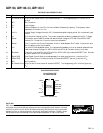
A simple N-channel FET can be used as an interface between
the overvoltage detect circuitry and the ADP1148 as shown in
Figure 16.
ADP1148
INT V
CC
C
T
5
4
VN2222LL
*FROM CROWBAR
DETECT CIRCUIT
*ACTIVE WHEN V
GATE
= VIN
OFF WHEN V
GATE
= GROUND
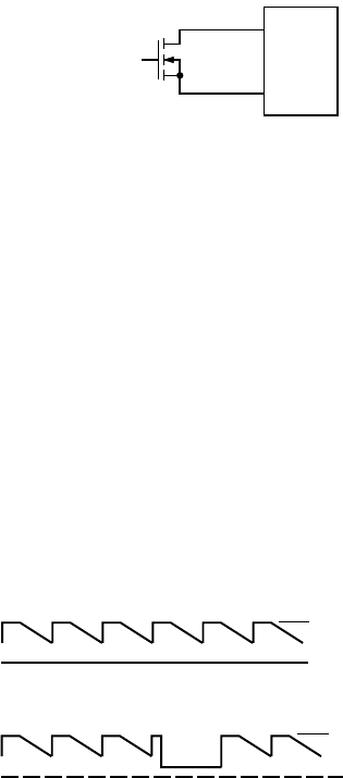
Figure 16. Output Crowbar Interface
Troubleshooting
Since efficiency is critical to ADP1148 applications, it is very
important to verify that the circuit is functioning correctly in
both continuous and power saving mode operation. The wave-
form to monitor is the voltage on the timing capacitor
C
T
pin.
In continuous mode (I
LOAD
> I
POWER SAVING MODE
), the voltage
on the C
T
pin should be a sawtooth with a 0.9 V
p-p swing. This
voltage should never dip below 2 V as shown in Figure 17a.
When load currents are low (I
LOAD
< I
POWER SAVING MODE
)
,
power
saving mode operation occurs. The voltage on the C
T
pin now
falls to ground for periods of time as shown in Figure 17b. If the
C
T
pin is observed falling to ground at high output currents, it
indicates poor decoupling or improper grounding. Refer to the
Board Layout list.
3.3V
0V
3.3V
0V
(A) CONTINOUS MODE OPERATION
(B) POWER-SAVING MODE
Figure 17. C
T
Waveforms