


ADP1148, ADP1148-3.3, ADP1148-5
–9–
REV. A
An additional 0.1 µF – 1 µF ceramic bypass capacitor is advised
on V
IN
Pin 3 parallel with C
IN
. The selection of C
OUT
is driven
by the required effective series resistance (ESR). The ESR of
C
OUT
must be less than twice the value of R
SENSE
for proper
operation of the ADP1148:
C
OUT
required ESR < 2 R
SENSE.
Optimum efficiency is obtained by making the ESR equal to
R
SENSE
. As the ESR is increased up to 2 R
SENSE
, the efficiency
degrades by less than 1%.
Manufacturers such as Sprague, and United Chemmicon should
be considered for high performance capacitors. The OS-CON
semiconductor dielectric capacitor has the lowest ESR for its
size, at a somewhat higher price. Once the ESR requirement for
C
OUT
has been met, the RMS current rating generally far ex-
ceeds the I
RIPPLE(P-P)
requirement.
In surface-mount applications multiple capacitors may have to
be paralleled to meet the capacitance, ESR, or RMS current
handling requirements of the application. Aluminum electrolytic
and dry tantalum capacitors are both available in surface-mount
configurations. In the case of tantalum, it is critical that the
capacitors are surge tested for use in switching power supplies.
Consult the manufacturer for other specific recommendations.
The C
O
output filter capacitor has to be sized correctly to avoid
excessive ripple voltages at low frequencies. See Figure 5 for
output capacitor selection.
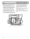
Transient Response
The regulator loop response can be checked by looking at the
load transient response. Switching regulators take several cycles
to respond to a step in dc (resistive) load current. When a load
step occurs, V
OUT
shifts by an amount equal to D1
LOAD
× ESR
,
where ESR is the effective series resistance of C
OUT.
D1
LOAD
also begins to charge or discharge C
OUT
until the regulator loop
adapts to the current change and returns V
OUT
to its steady-
state value. During this recovery time V
OUT
can be monitored
for overshoot or ringing which would indicate a stability prob-
lem. The external components on the I
TH
pin shown in the
Figure 1 circuit will prove adequate compensation for most
applications.
A second, more severe transient is caused by switching in loads
with large (>1 mF) supply bypass capacitors. The discharged
bypass capacitors are effectively put in parallel with C
OUT
, caus-
ing a rapid drop in V
OUT
. No regulator can deliver enough cur-
rent to prevent this problem if the load switch resistance is low
and it is driven quickly. The only solution is to limit the inrush
current to these capacitors below the current limit of the circuit.
Efficiency
The percent efficiency of a switching regulator is equal to the
output power divided by the input power times 100%. It is often
useful to analyze individual losses to determine what is limiting
the efficiency and which change would produce the most im-
provement. Percent efficiency can be expressed as:
% Efficiency = 100% - (L1 + L2 + L3 +. . . )
where L1, L2, etc. are the individual losses as a percentage of
input power. (For high efficiency circuits only small errors are
incurred by expressing losses as a percentage of output power.)
Although all dissipative elements in the circuit produce losses,
three main sources usually account for most of the losses in
ADP1148 circuits:
1) ADP1148 dc bias current,
2) MOSFET gate charge currents,
3) I
2
× R losses.
1) The dc supply current is the current which flows into V
IN
Pin
3 less the gate charge current. For V
IN
= 10 V the ADP1148
dc supply current is 160 µA for no load, and increases pro-
portionally with load up to a constant 1.6 mA after the
ADP1148 has entered continuous mode. Because the dc bias
current is drawn from V
IN
, the resulting loss increases with
input voltage. For V
IN
= 10 V the dc bias losses are generally
less than 1% for load currents over 30 mA. However, at very
low load currents the dc bias current accounts for nearly all
of the loss.
2) MOSFET gate charge currents result from switching the gate
capacitance of the power MOSFETs. Each time a MOSFET
gate is switched from low to high to low again, a packet of
charge dQ moves from V
IN
to ground. The resulting dQ/dt is
a current out of V
IN
which is typically much larger than the
dc supply current. In continuous mode, I
GATECHG
= f (Q
P
+
Q
N
). The typical gate charge for a 100 mΩ N-channel power
MOSFET is 25 nC and for the P-channel about twice that
value. This results in I
GATECHG
= 7.5 mA in 100 kHz continu-
ous operation for a 2% to 3% typical midcurrent loss with
V
IN
= 10 V.
Note that the gate charge loss increases directly with both
input voltage and operating frequency. This is the principal
reason why the highest efficiency circuits operate at moderate
frequencies. Furthermore, it argues against using a larger
MOSFET than necessary to control I
2
× R losses.
3) I
2
× R losses are easily predicted from the dc resistances of
the MOSFET, inductor, and current shunt. In continuous
mode the average output current flows through L and
R
SENSE
, but is “chopped” between the P-channel and N-
channel MOSFETs. If the two MOSFETs have about the
same R
DS(ON)
, the resistance of one MOSFET can be simply
summed with the resistances of L and R
SENSE
to obtain I
2
× R
losses. For example, if each R
DS(ON)
= 100 mΩ, R
L
= 150 mΩ,
and R
SENSE
= 50 mΩ, then the total resistance is 300 mΩ.
This results in losses ranging from 3% to 10% as the output
current increases from 0.5 A to 2 A. I
2
× R losses cause the
efficiency to roll-off at high output currents.
Figure 6 shows how the efficiency losses in a typical ADP1148
regulator. The gate charge loss is responsible for the majority of
the efficiency lost in the midcurrent region. If power saving
mode operation was not employed at low currents, the gate
charge loss alone would cause the efficiency to drop to unac-
ceptable levels. With power saving mode operation, the dc supply
current represents the lone (and unavoidable) loss component
which continues to become a higher percentage as output cur-
rent is reduced. As expected, the I
2
× R losses dominate at high
load currents. Other losses including C
IN
and C
OUT
ESR dissi-
pative losses, MOSFET switching losses, Schottky conduction
losses during deadtime and inductor core losses, generally
account for less than 2% total additional loss.